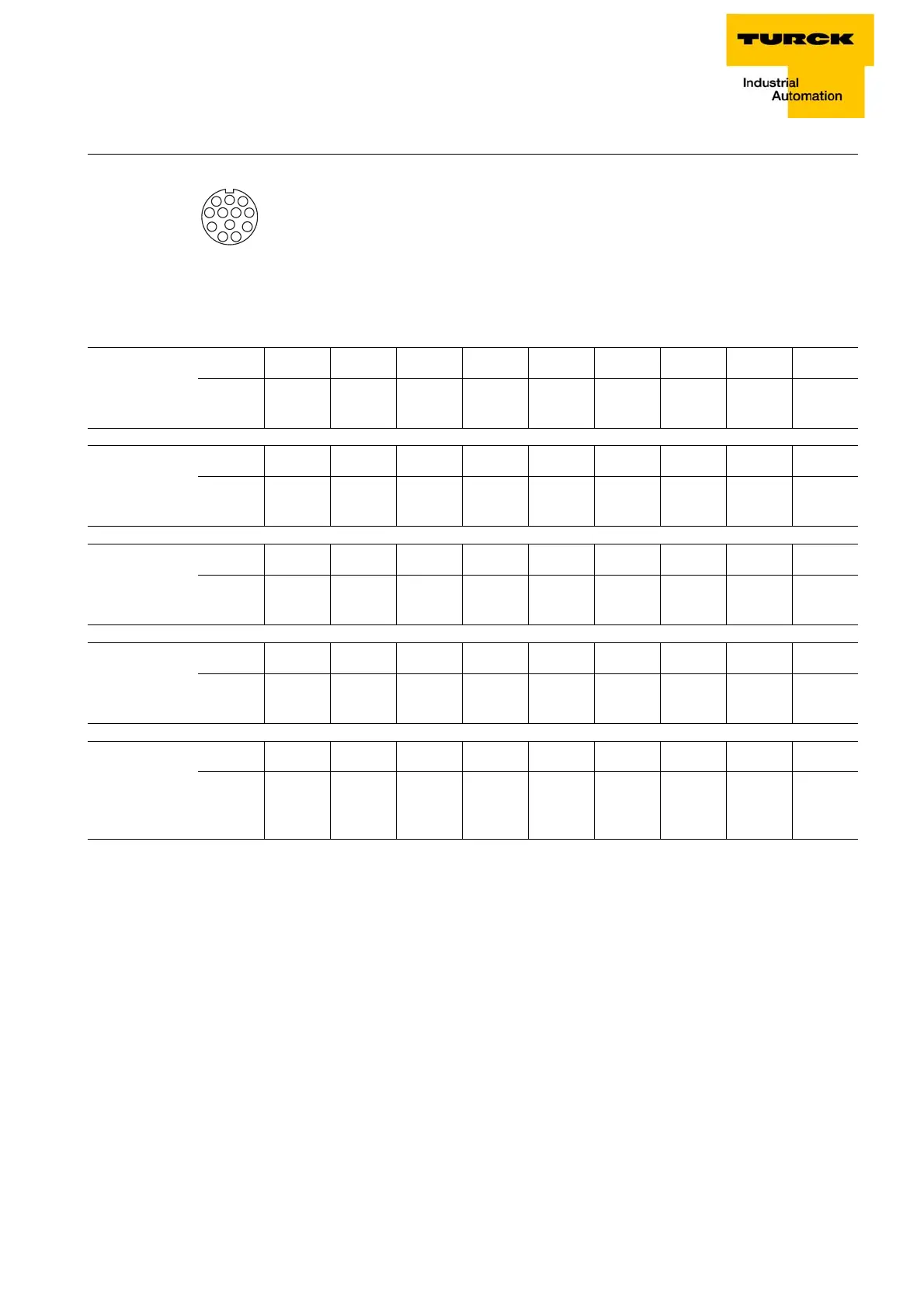
Figure 5-57:
81
9
712102
54
63
11
v
1 = Signal 0
2 = Signal 1
3 = Signal 2
4 = Signal 3
5 = n.c.
6 = n.c.
7 = n.c.
8 = n.c.
9 = V
SENS
10 = V
SENS
11 = V
SENS
12 = GND
D300529 0115 - BL67 I/O modules
5-39
BL67-4DI-N
5.6.6 Signal assignment
n = offset of input data; depending on extension of station and the corresponding fieldbus.
C = slot no.
P = pin no.
Pin assignment
BL67-4DI-N with
BL67-B-1M23
Table 5-39:
Signal assign-
ment
with BL67-B-
4M8
ByteBit 7Bit 6Bit 5Bit 4Bit 3Bit 2Bit 1Bit 0
In n - - - - C3P4 C2P4 C1P4 C0P4
Table 5-40:
Signal assign-
ment with BL67-B-
2M12
ByteBit 7Bit 6Bit 5Bit 4Bit 3Bit 2Bit 1Bit 0
In n - - - - C1P2 C0P2 C1P4 C0P4
Table 5-41:
Signal assign-
ment with
BL67-B-2M12-P
ByteBit 7Bit 6Bit 5Bit 4Bit 3Bit 2Bit 1Bit 0
In n - - - - C1P2 C1P4 C0P2 C0P4
Table 5-42:
Signal assign-
ment with
BL67-B-4M12
ByteBit 7Bit 6Bit 5Bit 4Bit 3Bit 2Bit 1Bit 0
In n - - - - C3P4 C2P4 C1P4 C0P4
Table 5-43:
Signal assignment
with
BL67-B-1M23
ByteBit 7Bit 6Bit 5Bit 4Bit 3Bit 2Bit 1Bit 0
In n - - - - C0P4 C0P3 C0P2 C0P1