A20 User Manual (Revision 1.2) Copyright © 2013 Allwinner Technology Co., Ltd. All Rights Reserved. Page 117 / 812
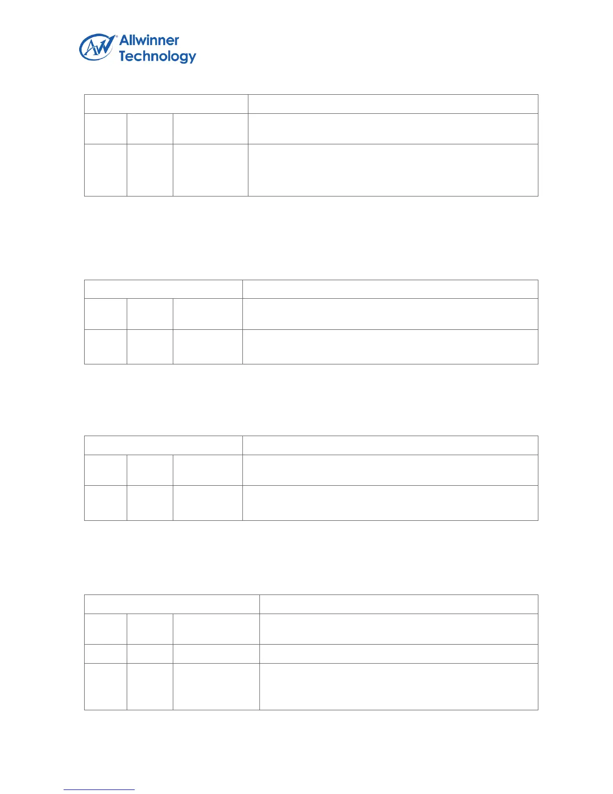
Register Name: TMR2_CTRL_REG
modified. If the timer is started again, and the Software hope
the current value register to down-count from the new interval
value, the reload bit and the enable bit should be set to 1 at
the same time.
Note: the time between the timer disabled and enabled should be larger than 2*Tcycles(Tcycles=
Timer clock source/pre-scale).
1.9.3.10. TIMER 2 INTERVAL VALUE REGISTER
Register Name: TMR2_INTV_VALUE_REG
TMR2_INTV_VALUE.
Timer 2 Interval Value.
Note: the value setting should consider the system clock and the timer clock source.
1.9.3.11. TIMER 2 CURRENT VALUE REGISTER
Register Name: TMR2_CUR_VALUE_REG
TMR2_CUR_VALUE.
Timer 2 Current Value.
Note: Timer current value is a 32-bit down-counter(from interval value to 0). This register can be read
correctly if the PCLK is faster than 2*TimerFreq(TimerFreq = TimerClkSource/pre-scale).
1.9.3.12. TIMER 3 CONTROL REGISTER(DEFAULT: 0X00000000)
Register Name: TMR3_CTRL_REG
TMR3_MODE.
Timer 3 mode.
0: Continuous mode. When interval value reached, the