A20 User Manual (Revision 1.2) Copyright © 2013 Allwinner Technology Co., Ltd. All Rights Reserved. Page 45 / 812
Register Name: PLL5_TUN_REG
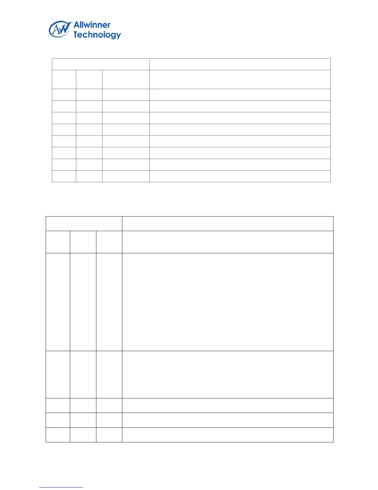
1.5.4.9. PLL6-SATA(DEFAULT: 0X21009911)
Register Name: PLL6_CFG_REG
PLL6_Enable.
0: Disable, 1: Enable.
There are two ouputs:
For SATA, the output =(24MHz*N*K)/M/6
If the SATA is on, the clock output should be equal to 100MHz;
For other module, the clock output = (24MHz*N*K)/2
PLL6*2 = 24MHz*N*K
Note: the output 24MHz*N*K clock must be in the range of
240MHz~2GHz if the bypass is disabled.
PLL6_BYPASS_EN.
PLL6 Output Bypass Enable.
0: Disable, 1: Enable.
If the bypass is enabled, the PLL6 output is 24MHz.