A20 User Manual (Revision 1.2) Copyright © 2013 Allwinner Technology Co., Ltd. All Rights Reserved. Page 49 / 812
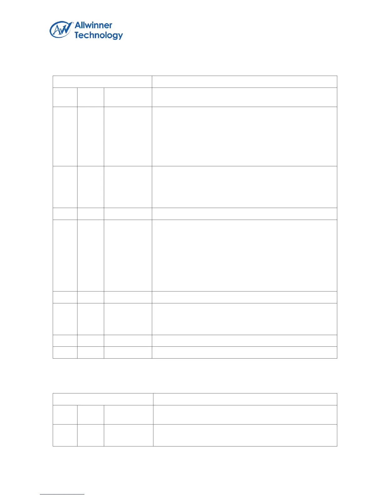
1.5.4.14. PLL8-GPU(DEFAULT: 0X21009911)
Register Name: PLL8_CFG_REG
PLL8_Enable.
0: Disable, 1: Enable.
The output = 24MHz*N*K
Note: the output 24MHz*N*K clock
must be in the range of 240MHz~2GHz if the bypass is
disabled.
PLL8_BYPASS_EN.
PLL8 Output Bypass Enable.
0: Disable, 1: Enable.
If the bypass is enabled, the PLL8 output is 24MHz.
PLL8_FACTOR_N.
PLL8 Factor N.
Factor=0, N=0;
Factor=1, N=1;
Factor=2, N=2;
……
Factor=31,N=31
PLL8_FACTOR_K.
PLL8 Factor K.(K=Factor + 1 )
The range is from 1 to 4.
1.5.4.15. OSC24M (DEFAULT: 0X00138013)
Register Name: OSC24M_CFG_REG
KEY_FIELD.
Key Field for LDO Enable bit.