A20 User Manual (Revision 1.2) Copyright © 2013 Allwinner Technology Co., Ltd. All Rights Reserved. Page 494 / 812
5.3.4.18. DEFE_WB_ADDR1_REG
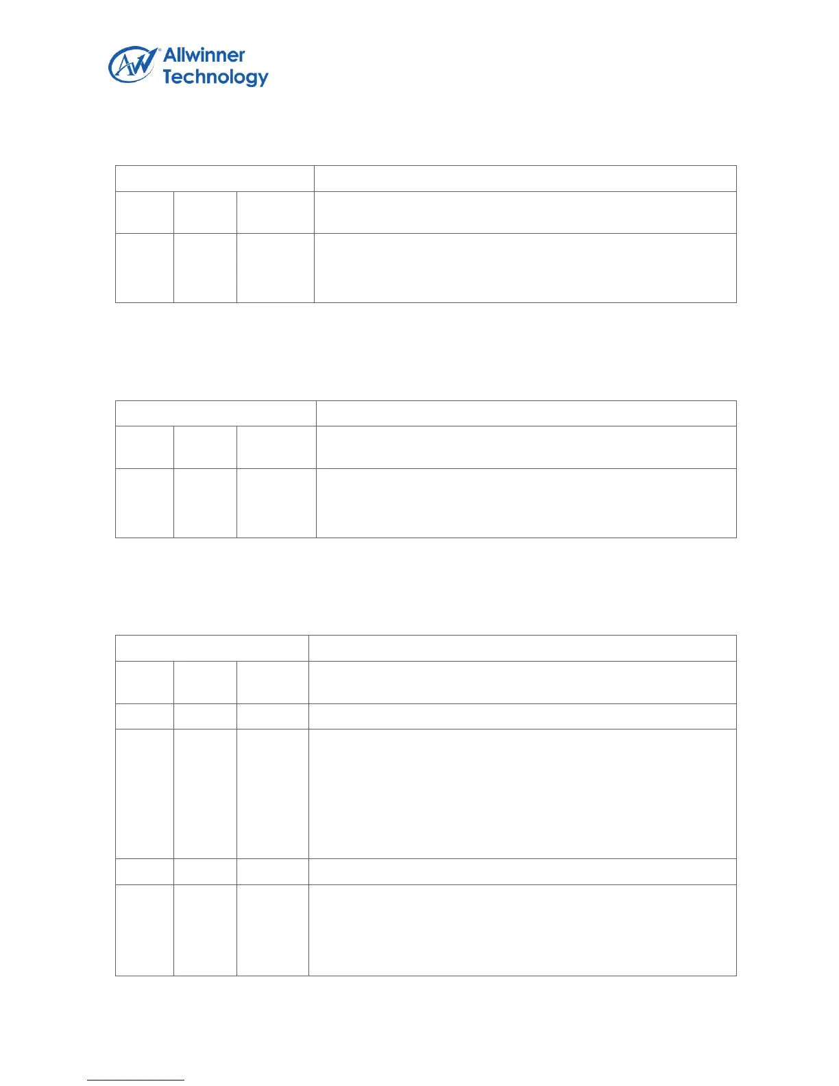
Register Name: DEFE_WB_ADDR1_REG
WB_ADDR
Write-back address setting for scaled data.
5.3.4.19. DEFE_WB_ADDR2_REG
Register Name: DEFE_WB_ADDR2_REG
WB_ADDR
Write-back address setting for scaled data.
5.3.4.20. DEFE_OUTPUT_FMT_REG
Register Name: DEFE_OUTPUT_FMT_REG
BYTE_SEQ
Output data byte sequence selection
0: P3P2P1P0(word)
1: P0P1P2P3(word)
For ARGB, when this bit is 0, the byte sequence is BGRA, and
when this bit is 1, the byte sequence is ARGB;
SCAN_MOD
Output interlace enable
0: disable
1: enable
 Loading...