A20 User Manual (Revision 1.2) Copyright © 2013 Allwinner Technology Co., Ltd. All Rights Reserved. Page 603 / 812
Register Name: SPI_DMACTL
Default Value: 0x0000_0000
6.3.4.7. SPI WAIT CLOCK REGISTER
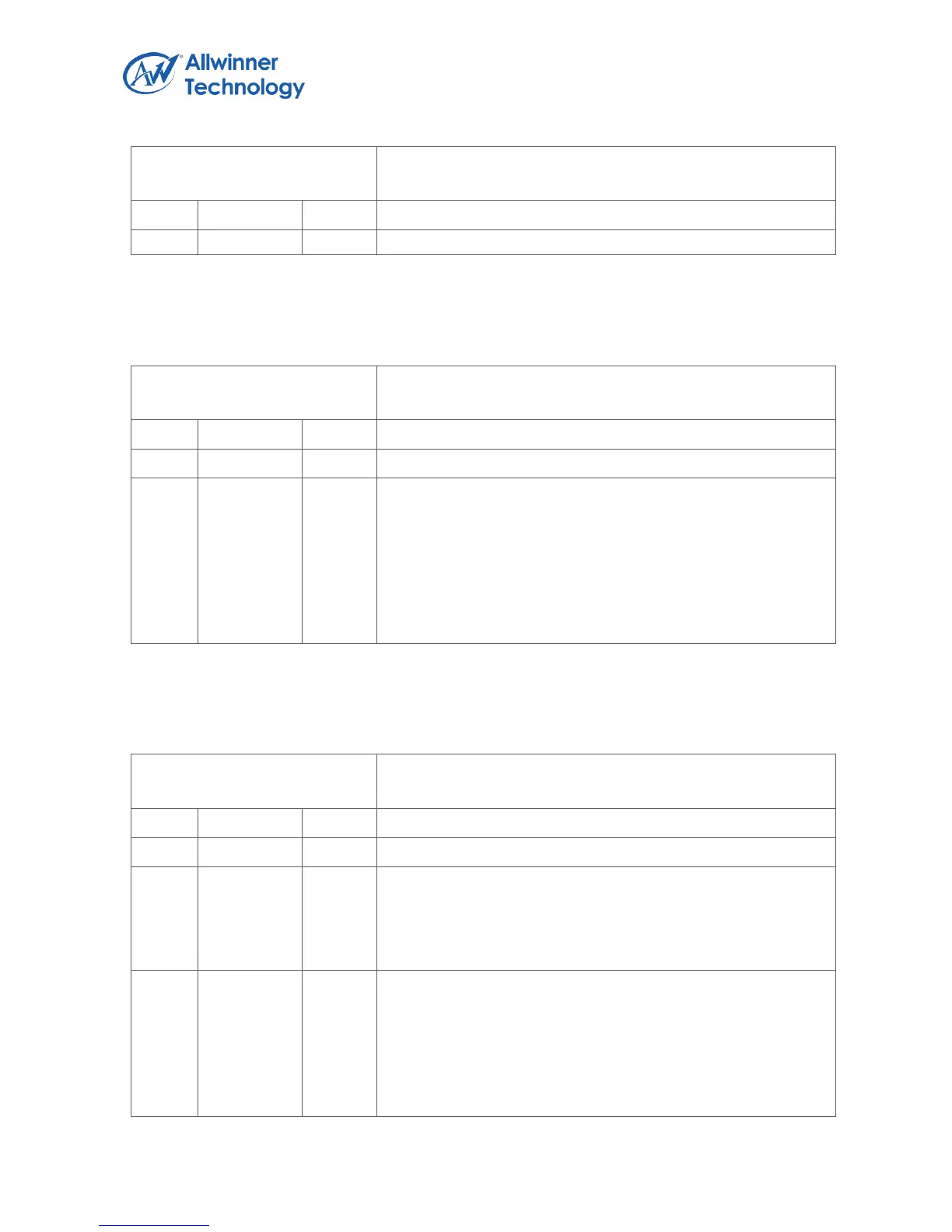
Register Name: SPI_WAIT
Default Value: 0x0000_0000
WCC
Wait Clock Counter (In Master mode)
These bits control the number of wait states to be inserted in
data transfers. The SPI module counts SPI_SCLK by WCC for
delaying next word data transfer.
0: No wait states inserted
N: N SPI_SCLK wait states inserted
6.3.4.8. SPI CLOCK CONTROL REGISTER
Register Name: SPI_CCTL
Default Value: 0x0000_0002
DRS
Divide Rate Select (Master Mode Only)
0: Select Clock Divide Rate 1
1: Select Clock Divide Rate 2
CDR1
Clock Divide Rate 1 (Master Mode Only)
This field selects the baud rate of the SPI_SCLK based on a
division of the AHB_CLK. These bits allow SPI to synchronize
with different external SPI devices. The max frequency is one
quarter of AHB_CLK. The divide ratio is determined according
to the following table using the equation: 2^(n+1). The
 Loading...