System Control
ARM DDI 0500D Copyright © 2013-2014 ARM. All rights reserved. 4-79
ID021414 Non-Confidential
Usage constraints This register is accessible as follows:
Configurations SDER32_EL3 is architecturally mapped to AArch32 register SDER. See
Secure Debug Enable Register on page 4-201.
Attributes SDER32_EL3 is a 32-bit register.
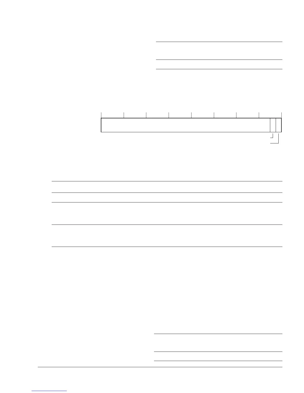
Figure 4-39 shows the SDER32_EL3 bit assignments.
Figure 4-39 SDER32_EL3 bit assignments
Table 4-78 shows the SDER32_EL3 bit assignments.
To access the SDER32_EL3:
MRS <Xt>, SDER32_EL3 ; Read SDER32_EL3 into Xt
MSR SDER32_EL3, <Xt> ; Write Xt to SDER32_EL3
4.3.44 Translation Table Base Register 0, EL1
The TTBR0_EL1 characteristics are:
Purpose Holds the base address of translation table 0, and information about the
memory it occupies. This is one of the translation tables for the stage 1
translation of memory accesses from modes other than Hyp mode.
Usage constraints This register is accessible as follows:
EL0
EL1
(NS)
EL1
(S)
EL2
EL3
(SCR.NS = 1)
EL3
(SCR.NS = 0)
-- --RW RW
Table 4-78 SDER32_EL3 bit assignments
Bits Name Function
[31:2] - Reserved,
RES0.
[1] SUNIDEN Secure User Non-invasive Debug Enable The possible values are:
0
Non-invasive debug not permitted in Secure EL0 mode. This is the Warm reset value.
1
Non-invasive debug permitted in Secure EL0 mode.
[0] SUIDEN Secure User Invasive Debug Enable. The possible values are:
0
Invasive debug not permitted in Secure EL0 mode. This is the Warm reset value.
1
Invasive debug permitted in Secure EL0 mode.
EL0
EL1
(NS)
EL1
(S)
EL2
EL3
(SCR.NS = 1)
EL3
(SCR.NS = 0)
- RWRWRWRW RW