System Control
ARM DDI 0500D Copyright © 2013-2014 ARM. All rights reserved. 4-228
ID021414 Non-Confidential
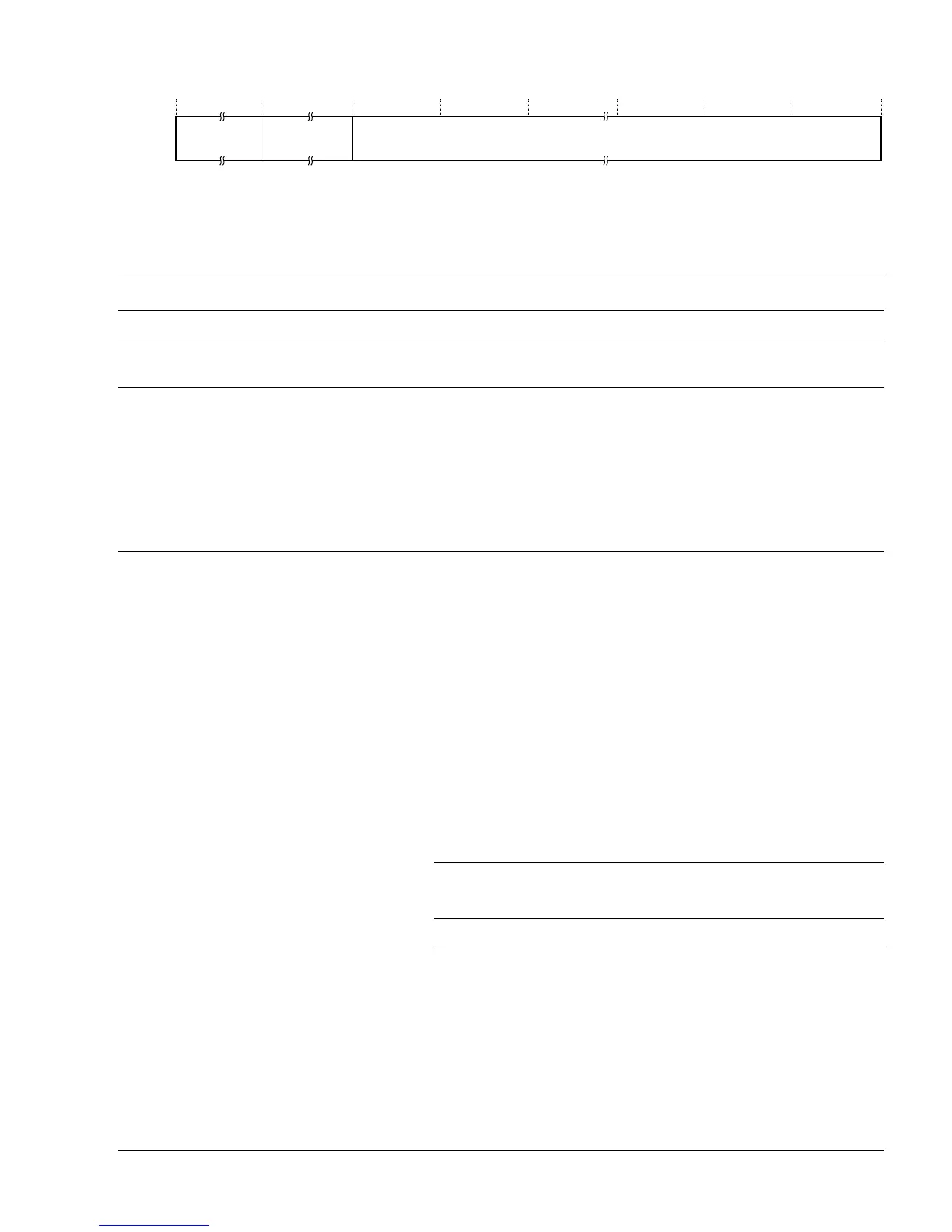
Figure 4-114 TTBR1 bit assignments, TTBCR.EAE is 1
Table 4-209 shows the TTBR1 bit assignments when TTBCR.EAE is 1.
To access the 64-bit TTBR1 when TTBCR.EAE = 1:
MRRC p15, 1, <Rt>, <Rt2>, c2 ; Read 64-bit TTBR1 into Rt (low word) and Rt2 (high word)
MCRR p15, 1, <Rt>, <Rt2>, c2 ; Write Rt (low word) and Rt2 (high word) to 64-bit TTBR1
4.5.42 Translation Table Base Control Register
The TTBCR characteristics are:
Purpose Determines which of the Translation Table Base Registers defined the
base address for a translation table walk required for the stage 1 translation
of a memory access from any mode other than Hyp mode. Also controls
the translation table format and, when using the Long-descriptor
translation table format, holds cacheability and shareability information.
Usage constraints This register is accessible as follows:
The processor does not use the implementation-defined bit, TTBCR[30],
when using the Long-descriptor translation table format, so this bit is
RES0.
Configurations TTBCR (NS) is architecturally mapped to AArch64 register TCR_EL1.
See Translation Control Register, EL1 on page 4-86.
There are separate Secure and Non-secure copies of this register.
Table 4-209 TTBR1 bit assignments, TTBCR.EAE is 1
Bits Name Function
[63:56] - Reserved,
RES0.
[55:48] ASID An ASID for the translation table base address. The TTBCR.A1 field selects either TTBR0.ASID or
TTBR1.ASID.
[47:0] BADDR[47:x] Translation table base address, bits[47:x]. Bits [x-1:0] are
RES0.
x is based on the value of TTBCR.T0SZ, and is calculated as follows:
• If TTBCR.T0SZ is 0 or 1, x = 5 - TTBCR.T0SZ.
• If TTBCR.T0SZ is greater than 1, x = 14 - TTBCR.T0SZ.
The value of x determines the required alignment of the translation table, that must be aligned to 2x bytes.
If bits [x-1:3] are not all zero, this is a misaligned Translation Table Base Address. Its effects are
CONSTRAINED UNPREDICTABLE, where bits [x-1:0] are treated as if all the bits are zero. The value read
back from those bits is the value written.
EL0
(NS)
EL0
(S)
EL1
(NS)
EL1
(S)
EL2
EL3
(SCR.NS = 1)
EL3
(SCR.NS = 0)
- - RWRWRWRW RW