APPLIC ATION BLO CKS 165
12 APPLICATION BLOCKS
The PL/X contains a comprehensive range of extra system application blocks. These are described in a
separate accompanying manual. At the time of publication, the list of blocks is as follows
APPLIC A TIO N BLO CKS / SUMMER 1, 2
APPLIC A TION BLO CKS / PID 1, 2.
APPLIC A TION BLO CKS / PARAMETER PROFILER
APPLIC A TION BLO CKS / REEL DIAMETER CALC
APPLIC A TION BLO CKS / TAPER TENSION C ALC
APPLIC A TION BLO CKS / TORQUE C O MPENS A T OR
APPLIC A TION BLO CKS / PRESET SPEED
APPLIC A TION BLO CKS / MULTI-FUNC TION 1 to 8
APPLIC A TIO N BLO CKS / LATCH
APPLIC A TION BLO CKS / FILTER 1, 2
APPLIC A TION BLO CKS / BA TCH CO UNTER
APPLIC A TIO N BLO CKS / INTERV AL TIMER
APPLIC A TION BLOCKS / CO MPARATOR 1 to 4
APPLIC A TION BLOCKS / C/O SWIT CH
12.1 Ge neral rules
12.1.1 Sample times
When application blocks are being processed the
workload on the internal microprocessor is increased.
With no application blocks activated the time taken to
perform all the necessary tasks (cycle time) is
approximately 5mS.
With al l the application blocks activated the cycle time
is approximately 10mS. In the future the designers
expect to add even more application blocks. It is not
expected ho w ever that the typical cycle time will ever be greater than 30mS. (Bear in mind that it w ould be
highly unusual for all the application blocks to be activated). With this in mind it is recommended that the
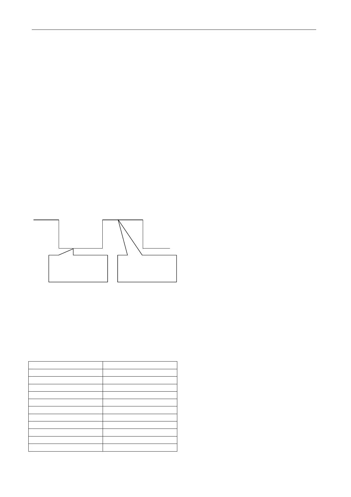
system designer takes care that external logic signals are stable long enough to be recognised. In order to
achieve this, the logic input minimum dw ell time has been specified at 50mS. How ever it will of course be
possible to operate with much lower d well times than this for specific installations where the cycle time is
lo w. There is then ho w ever the risk that a future re-configuration of the blocks by the user would increase
the cycle time sufficiently to cause sampling problems.
12.1.2 Order of processing
It may be useful for system designers to kno w the order in which the blocks are processed within each cycle.
0) Analogue inputs 12) Torque compensator
1) Motorised pot 13) Zero interlocks
2) Digital inputs 14) Speed control
3) Reference exchange 15) Preset speed
4) Jumpers 16) Parameter profile
5) Multi-function 17) Latch
6) Alarms 18) Batch counter
7) PID1, 2 19) Interval timer
8) Summer 1, 2 20) Filters
9) Run mode ramps 21) Comparators
10) Diameter calc 22) C/O Switches
11) Taper tension 23) All terminal outputs
The input low
time must be at
least 50mS
The input high
time must be at
least 50mS