Introduction and Technical Data 27
0 volts
I arm
I field A VF 5.12 V
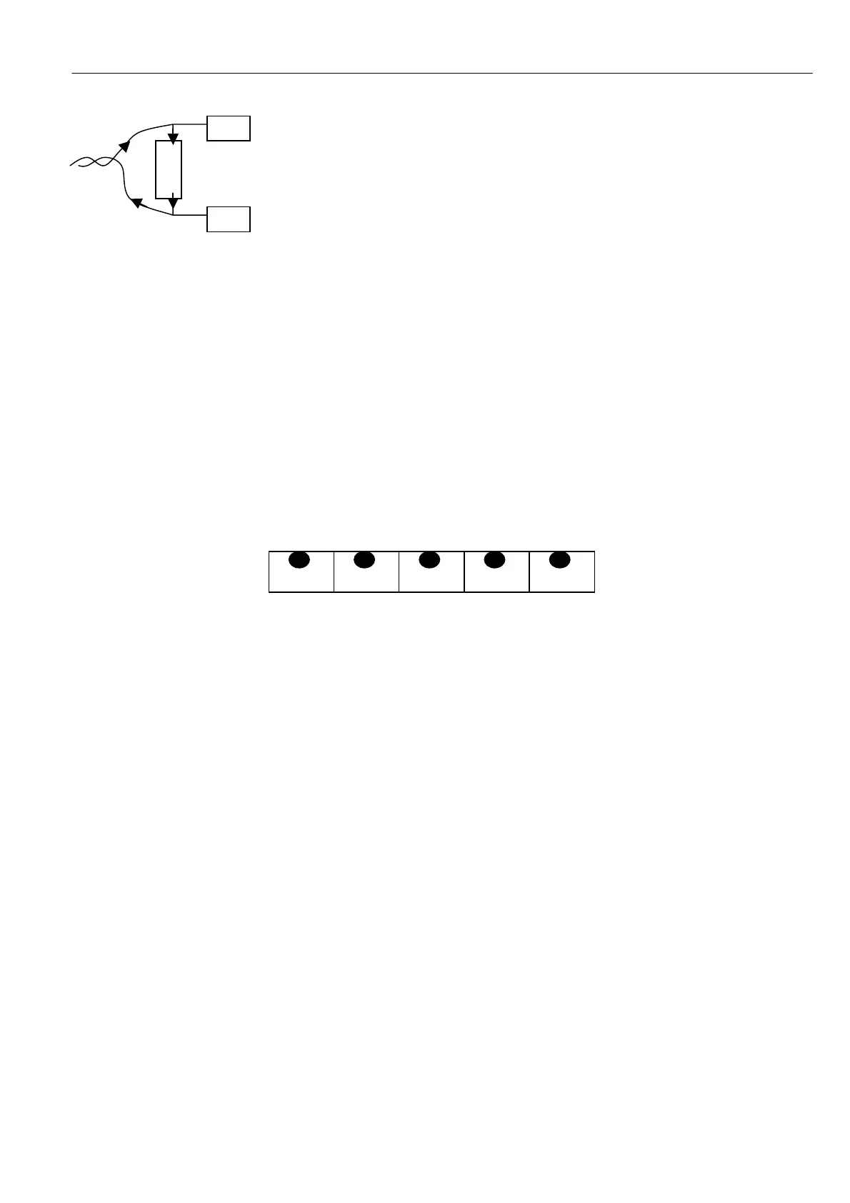
When using 4-20mA loop signals all that is required is to fit an external burden
resistor of 22 0 Ohms between the input and 0 V. Then set up the relevant UIP to
read the resulting voltage signal generated by passing the signal current through
the burden. The diagram sho ws a 4-20m A signal flowing through an external
burden resistor.
See 13.3.1.2.1 4-20mA loop input SETUP
3.4.4 Analogue tachogenerator input
This input is intended solely for the connection of an analogue bi-polar DC tachogenerator. An A C
tachogenerator with a rectified output may also be used with the PL series 2 quadrant drives. Terminals T25
0V and T 26 T A CH should be used for the t wo connections to the tachogenerator. A DC voltage of up to + /-
200V DC maximum can be applied directly to T26 with respect to T25.
See 6.1.9 C ALIBRATIO N / Speed feedback type PIN 9 QUICK START, to select tach feedback, and 6.1.8
C ALIBRA TION / Max tacho volts PIN 8, to match the 100% feedback voltage and sign on T26.
For forward motor rotation corresponding to a positive reference signal, the tachogenerator feedback voltage
sign at terminal T2 6 with respect to T25 (O V) must correspond to the sign selected in the calibration menu.
The programming facility allows selection of feedback voltages down to 0V, how ever it is not advisable in
the interest of accuracy and smooth operation to use tachos with a voltage less than 10 V at full speed.
3.4.5 Signal test pins
There is a row of test pins just behind the middle control terminal used to monitor certain feedback signals.
The Iarm signal is an attenuated unfiltered inverted version of terminal 29, and may be used to observe the
current response of the PL/X. See 13.13.3 DRIVE PERSON ALIT Y / Maximum current response PIN 67 8.
See 13.4.1 ANALO G OU TPUTS / A OP4 Iarm output rectify enable PIN 250.
Signal sign and amplitude is 0 to -/ + 2V linear output for 0 to + /-100% model rating current (inverted) for
unrectified mode, or 0 to -2V linear output for 0 to + /-100 % model rating current for rectified mode.
The other signals are intended for factory use only.
3.5 Control terminal default functions
When the drive is shipped the control terminals are allocated with default functions. These are chosen to be
as generally useful as possible in most applications. All the programmable terminals are available to be re-
allocated to an alternative function by the user if desired.
This is a list of the default functions. Note if after programming you wish to return the drive to this default
function set up, then arrange to have all 4-menu keys depressed simultaneously during the application of
control power. See 5.1.3 Restoring the drive parameters to the default condition, and see 13.13.2 DRIVE
PERSONALITY / Recipe page PIN 677.
OV terminal 0V T1
Aux. Speed Reference Analogue Input UI P2 T2
0 to + /-10 V linear input for 0 to + /-100 % speed. Overvoltage protected to + /-50V. Input impedance 100K.
Speed Reference/Current dema nd Analogue Input UIP3 T3
0 to + /-10V linear input for 0 to + /-100% speed. Overvoltage protected to + /-50 V. Input impedance 100K.
(Note, this analogue input is sampled faster than the others for very rapid response applications. E. g. as a
current reference. See 6.7.1 SPEED CONTROL / Block diagram).
See 6.7.7.7 SPEED PI A D APTION / Using small speed inputs. The default gives lo w gain for small inputs.