Intel740™ Graphics Accelerator Design Guide
2-9
Addin Card Design
2.2.3.2 Ground Connections
All lands in the four corners and center are V
ss
(GND). Thermal analysis requires that each V
ss
ball
connect to an adjacent via which passes through to the solder side of the board, one via per ball,
with a trace as wide as the via. Heat will dissipate through these vias to the GND plane as well as to
the air on the solder side.
2.2.3.3 Power Connections
The VCC2 plane should be as wide as practical for high current-carrying capacity. Because of the
interspersing of VCC2 and VCC3 pins on the Intel740™ graphics accelerator, a polygon will be
needed on one of the signal layers to extend the VCC3 plane to the isolated VCC3 pins
(Figure 2-9). The VCC2 polygon is a separate plane on the VCC Layer; the darker VCC3 polygon
is a power flood on the solder side and connects to the VCC3 plane on the VCC Layer through vias.
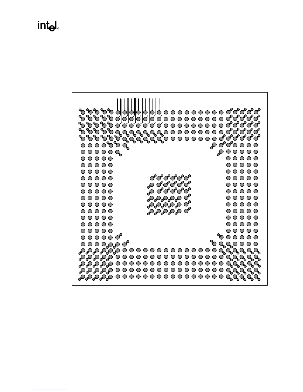
Figure 2-8. Dogbone Via Pattern