Revision 0.9
21
PC SGRAM Specification
9.0 SGRAM AC/DC Parameters
9.1 DC Specifications for 100-166 MHz
NOTES:
1. Input leakage currents include hi-Z output leakage for all bi-directional buffers with tri-state outputs.
2. This is a recommendation, not an absolute requirement. The actual value should be provided with the
component data sheet.
9.2 A.C. Specifications for 100-166 MHz
NOTES:
1. The overshoot and undershoot voltage duration is <=3ns with no input clamp diodes
2. The VDDQ and VSSQ are the operating parameters (not absolute max. parameters)
The refresh rate for all devices is assumed at a maximum of 15.6us per row per
the table below.
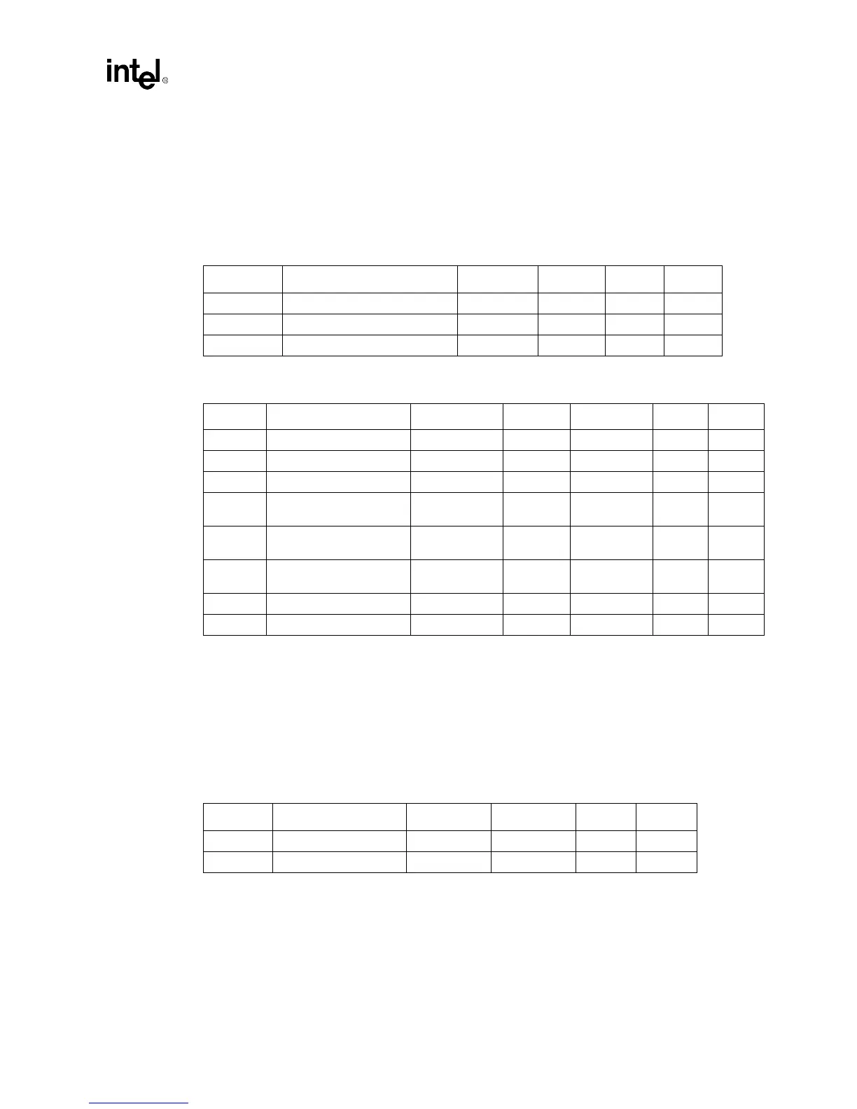
Table 9. Absolute Maximum D.C. Rating
Symbol Parameter Min Max Units Notes
Vin, Vout Voltage on any pin w.r.t V
SS
-0.5 V
DD
+ 0.5 V
V
DD
, V
DDQ
Voltage Supply pins pin w.r.t V
SS
-0.5 4.5 V
Ts Storage Temperature -55 125
°
C
Table 10. D.C Operating Requirements
Symbol Parameter Condition Min Max Units Notes
VDD Supply Voltage 3.135 3.6 V
VDDQ I/O Supply Voltage 3. 135 3.6 V
Iil Input Leakage Current 0 < Vin < VDDQ -10 +10
µ
A1,2
Cin Input Pin Capacitance @1MHz 2.5 5.0 pF
Target
3.75pf
CI/O I/O Pin Capacitance @1MHz 4.0 6.5 pF
Target
5.25pf
Cclk Pin Capacitance @1MHz 2.5 4.0 pF
Target
3.25pf
Lpin Pin Inductance 10 nH 2
Ta Ambient Temperature No Airflow 0 65
°
C
Table 11. Maximum AC Operating Requirements
Symbol Parameter Min Max Units Notes
Vih Input High Voltage 2.0 VDDQ+2.0 V 1,2
Vil Input Low Voltage VSSQ
−
2.0 0.8 V 1,2