Revision 0.91
5
SO-DIMM Module — Unbuffered SDRAM/SGRAM Graphics
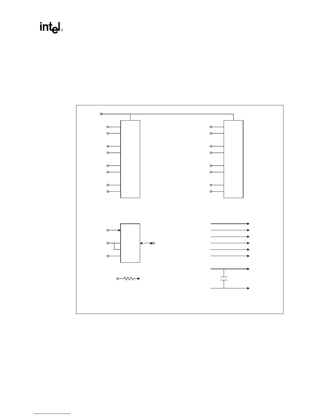
5.0 Graphics SO-DIMM Block Diagram
Figure 2 through Figure 5 illustrate the electrical connectivity of several SO-DIMM configurations.
The series termination resistors on CLK0 and CLK1 are not currently used and should be set to 0
ohms. Table 3 “Address Translation” on page 9 should be followed for connecting 256Kx32 and
512Kx32 devices.
Figure 2. 256K/512 x 64 SGRAM SO-DIMM Block Diagram (1 bank of two 256K/512K x 32)
DQM0
DQ[7:0]
DQM1
DQ[15:8]
DQM2
DQ[23:16]
DQM3
DQ[31:24]
512Kx32
Or
256Kx32
SGRAM
D0
CS
CS0
DQM4
DQ[39:32]
DQM5
DQ[47:40]
DQM6
DQ[55:48]
DQM7
DQ[63:56]
512Kx32
Or
256Kx32
SGRAM
D1
CS
SCL
VSS
SBA
A2
A1
A0
CLK0 D0, D1
Serial
PD
(optional)
SDA
CKE D0 to D1
D0 to D1/RAS
/CAS D0 to D1
D0 to D1/WE
DSF D0 to D1
D0 to D1A[10:0]
VCC
VSS
D0 to D1
D0 to D1
Three bypass capacitors per
SGRAM device (refer to
component section).
A001.vsd