3 Device AGP MotherBoard Design
3-20
Intel740™ Graphics Accelerator Design Guide
Table 3-14. Memory Layout Restrictions (See Figure 3-19)
Note: It is important to match clock lengths. For example, if the length from OCLK to Resistor is 1.03,
then the length from Resistor to RCLK should be 3.03 (OCLOCK to Resistor + 2’’).
Figure 3-18. Layout Dimensions (WEA#, SRASA#, SCASA#, CSA0#)
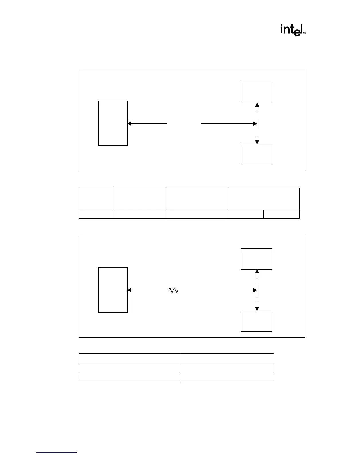
Table 3-13. Memory Layout Restrictions (See Figure 3-19)
Signal Intel740™ to Resistor Resistor to SGRAM Stub SGRAM Stub
Min Max
TCLK1 0.6” 3.4” ±0.25” 0.4” 0.6”
Figure 3-19. Memory Layout Dimensions (TCLK1)
Signal Intel740™ to Resistor
OCLK to Resistor 1.0” ±0.25
RCLK0, RCLK1 3.0” ±0.25”
Intel740™
Chip
2.25" - 4.9"
SGRAM
SGRAM
0.25" - 0.6"
0.25" - 0.6"
Intel740™
Chip
0.6"
SGRAM
SGRAM
0.4" - 0.6"
0.4" - 0.6"
3.4" ± 0.025"
0