3 Device AGP MotherBoard Design
3-16
Intel740™ Graphics Accelerator Design Guide
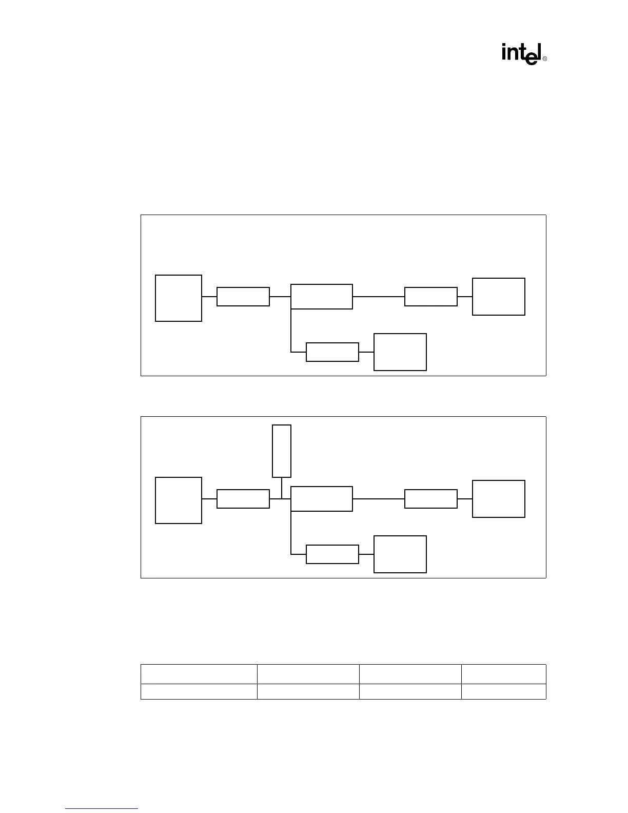
3.2.3.6 3-Load AGP Topology
Figure 3-11 and Figure 3-12 show the topologies for a 3-load AGP bus. The motherboard is
divided into 2 trace segments as shown. These are referred to as segment A and B. The
motherboard contains one AGP connector and one AGP master device. In the case of the strobe
signals, a 3
rd
segment was added to represent the stub lengths of the pull up resistors. This segment
is referred to as segment D. The net scheduling for this topology is segment A to connector,
connector to segment B.
3.2.3.7 Overall Solution Space
Two solution spaces were found. Selecting the appropriate solutions is dependent on the 82443BX
placement relative to the AGP connector. Solution 1 was implemented on this design.
Solution 1. Note that A + B within a group must be matched by 0.5”. Example:
Figure 3-11. 3 Device Data Load Topology
82443BX Segment A Connector
Segment B
Intel740™
Chip
Segment C
AGP
Master
Motherboard Add - In Card
Figure 3-12. 3 Device Strobe Load Topology
82443BX Segment A Connector
Segment B
Intel740™
Chip
Segment D
Segment C
AGP
Master
Motherboard Add - In Card
Table 3-8. Strobe and Data Segment Solution Space
Solution segment A Segment B Segment D
solution 1 3.5” - 5.5” * 2.0” - 3.0” 0.4” - 0.9”