3 Device AGP MotherBoard Design
3-4
Intel740™ Graphics Accelerator Design Guide
allows it to be put in a low power state. In this low power state, the Intel740 chip is disabled and
will not initiate or respond to cycles on the AGP bus. In addition, the power consumption of this
device in this state is less than 1 Watt. To put the Intel740 chip into the low power mode, the
following sequence of events must occur in the order stated.
1. ROMA16 must be asserted (high) at the trailing edge of the Intel740 chip RESET#
2. At least one AGP/Core clock before TEST is asserted the following signals must driven to the
state listed in Table 3-1
3. TEST is asserted (asserted =high = 1)
3.1.4.2 Low Power Logic Implementation
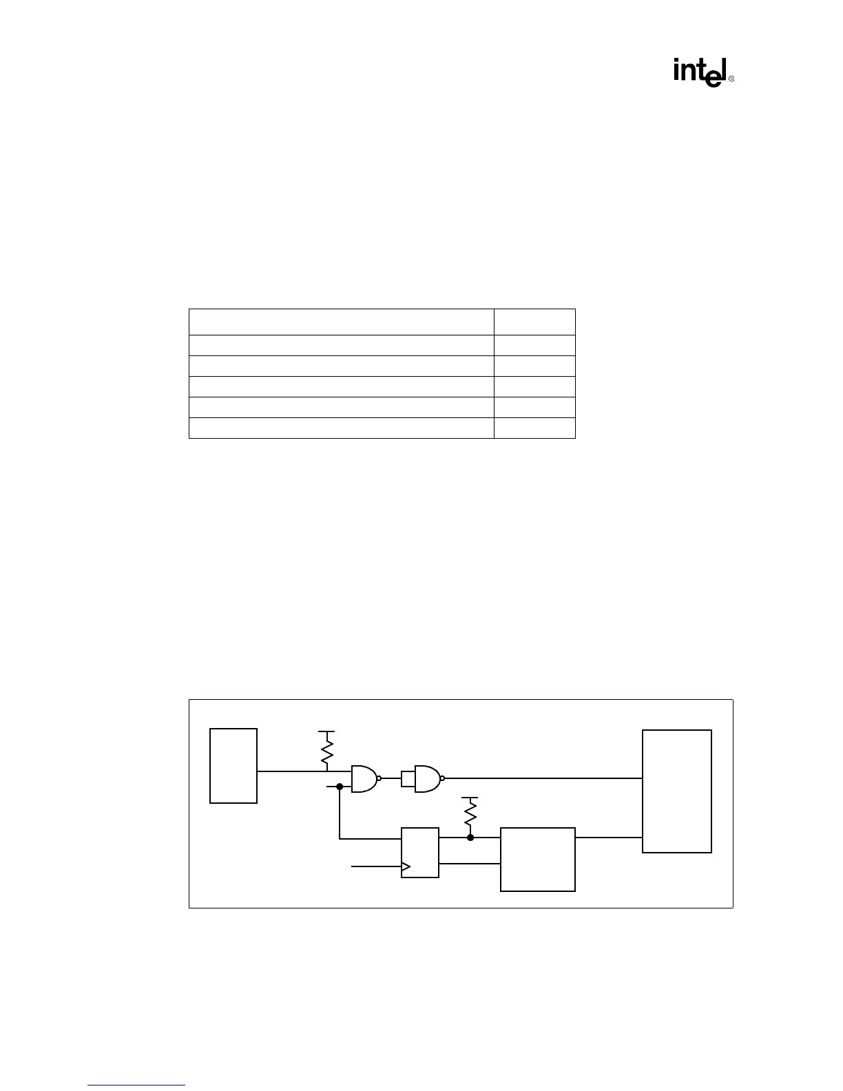
Two signals, GPO27# and GPO 28#, from the PIIX4E are used in this design. GPO28 in
conjunction with ROMA16 and PCIRST# are used to put the Intel740 chip in low power mode (see
Figure 3-2). The additional logic for driving WEB#, SCASB#, SRASB#, CS0B#, CS1B# and
TEST is illustrated in Figure 3-2.
A hardware reset to the Intel740 chip takes the device out of the low power state. Since the
PCIRST# signal is used to disable the device, it can not be used for this purpose. GPO27 serves as
the hardware reset to reset the Intel740 chip. At the trailing edge of GPO27, the Intel740 chip will
be functional.
Table 3-1. State of Signals to be Driven After System Reset but at Least One Clock Prior to
Asserting TEST
Signal State
WEB# 0
SCASB# 1
SRASB# 0
CS0B# 0
CS1B# 0
Figure 3-2. The Schematic Diagram for GPO27#, PCIRST# (System Reset), RESET#, ROMA16
Signals
PIIX4E
PCIRST#
GPO27#
Vcc3
D
Q
Q#
PCICLK3
Vcc3
OE#
IN1 OUT1
ROMA16
RESET
Intel740™
Chip
4.7 K
Ω
4.7 K
Ω