Intel740™ Graphics Accelerator Design Guide
2-11
Addin Card Design
2.2.3.5 General Signal Routing
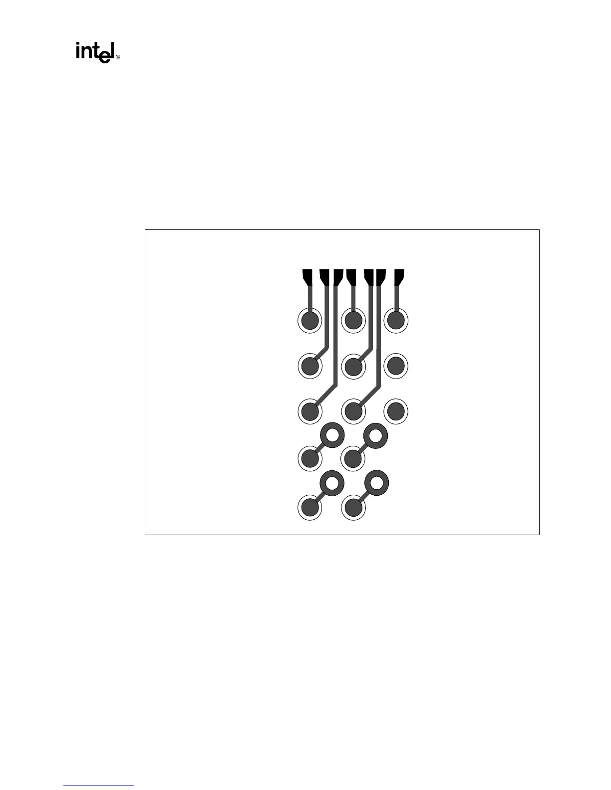
Figure 2-11 depicts general escape of traces from the five rows of BGA ball pads. The first three
ball rows can be routed on the primary layer. The last two must be routed through vias to the
secondary layer. Underneath the BGA, trace routing should be 5 on 5 or 6 on 6. Once the traces
have left the BGA, however, routing should expand to 5 on 10 or 6 on 12. The ratio should be kept
as 1:2.
The signals AD_STB_A, AD_STB_B and SB_STB should have a spacing of 1:4 to other signals.
Using this extra spacing between these specific signals will help to keep crosstalk to a minimum.
2.2.4 Voltage Regulator
The physical tab (used as a built in heatsink) on the MOSFET package is the drain pin, and will
need a tab-shaped pad to solder to.
Note: The resistor/capacitor network between the COMP pin (pin 5) and the GND pin (pin 3) of the
LT1575 should be connected directly to the GND pin of the device rather than tied to the ground
plane.
2.2.5 Bt829 Video Decoder
Note: Rockwell* Semiconductor should be contacted for up to date layout recommendations.
Figure 2-11.
Intel740™ Graphics Accelerator BGA Routing Exampl
e
COMPONENT SIDE ROUTING FOR 5 ROWS OF BALL PADS
R5
R4
R3
R2
R1