Addin Card Design
2-14
Intel740™ Graphics Accelerator Design Guide
For example, AD29 and AD_STB_B must not be mismatched by more than 0.5”. No such
comparison, however, should be enforced between AD29 and AD30, or AD29 and C/BE2#, etc.
Note: AGP strobes must be separated by 2X normal signal spacing (i.e., if normal spacing is 5/10 or 6/12,
the strobe signals must be separated from other traces by 20 or 24 mils, respectively).
2.2.6.5 Intel740™ Graphics Accelerator Memory Layout and Routing
Guidelines
The Intel740 graphics accelerator integrates a memory controller which supports a 64-bit memory
data interface. SGRAM can be used in addition to SDRAM if it is configured to perform as an
SDRAM. The Intel740 graphics accelerator generates the Row Address Strobe (SRAS[A:B]#),
Chip Selects (CS0[A:B]#, CS1[A:B]#), Column Address Strobe (SCAS[A:B]#), Byte Enables
(DQM[0:7]#), Write Enables (WE[A:B]#), and Memory Addresses (MA). The memory controller
interface is fully configurable through a set of control registers.
Eleven memory address signals (MAx[10:0]) allow the Intel740™ graphics accelerator to support
a variety of commercially available SO-DIMMs and components. Two SRAS# lines permit two
64-bit wide rows of SDRAM. All write operations must be one Quadword (QWord). The Intel740
graphics accelerator supports memory up to 100 MHz.
Rules for populating a Intel740 graphics accelerator Memory:
•
Memory can be populated using either an SO-DIMM or components.
•
SDRAM and SGRAM components and/or SO-DIMMs can be mixed.
•
The DRAM Timing register, which provides the DRAM speed grade control for the entire
memory array, must be programmed to use the timings of the slowest memories installed.
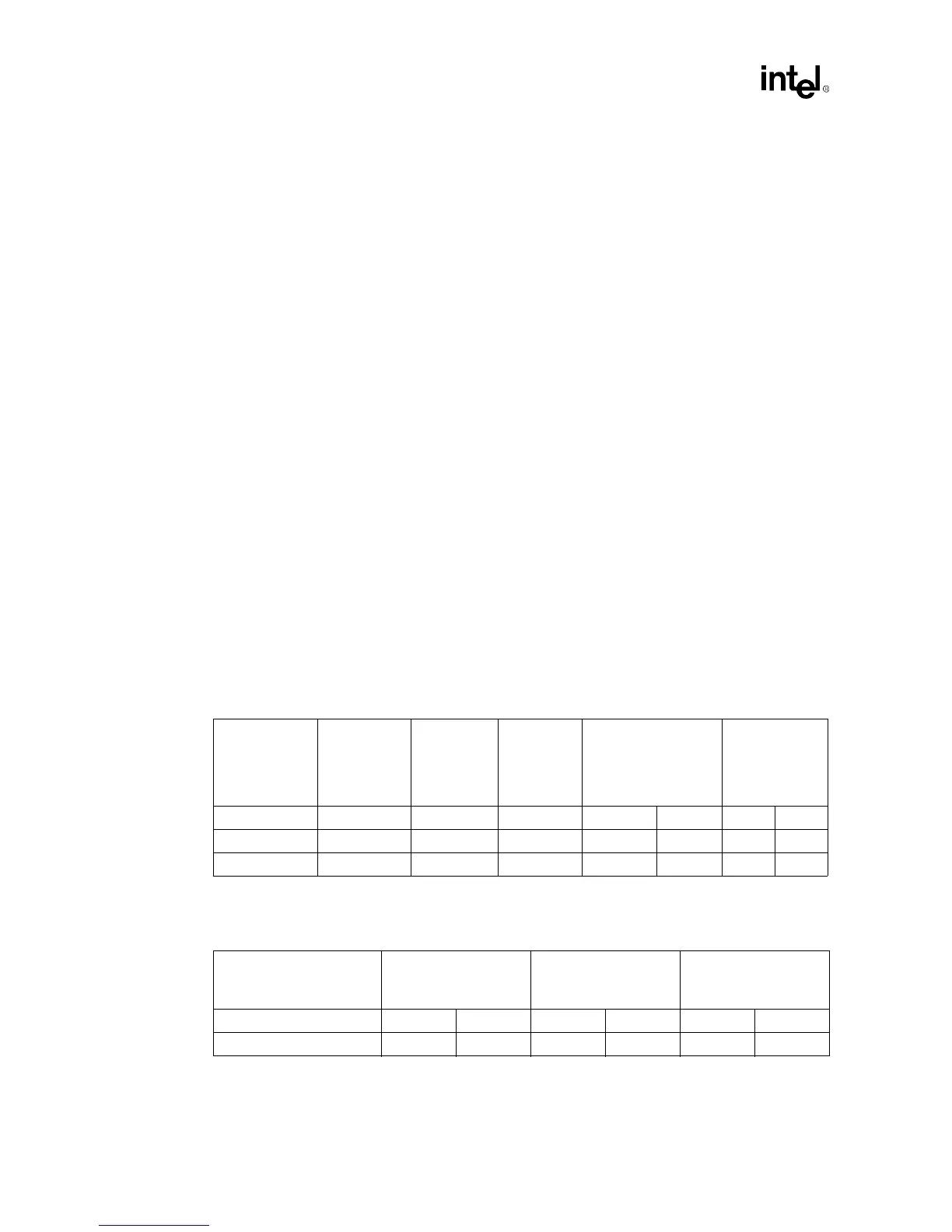
Possible DRAM and system options supported by the Intel740 graphics accelerator are shown in
Table 2-8.
There are several groups of signals within the memory bus with layout restrictions.
Table 2-8. Supported Memory Options (Other Memory Options Are Not Supported)
SDRAM/
SGRAM
Technology
SDRAM/
SGRAM
Density
SDRAM/
SGRAM
Width
Addressing Address Size
Local Memory
Size
Row Column Min Max
8 Mbit 256K 32 Asymmetric 10 8 2MB 4MB
16Mbit 512K 32 Asymmetric 11 8 4MB 8MB
16Mbit 1M 16 Asymmetric 12 8 8MB 8MB
Table 2-9. Memory Layout Restrictions (See Figure 2-12 and Figure 2-13)
Signal Intel740™ to SO-DIMM SO-DIMM SGRAM Stub SGRAM Stub
Min Max Min Max Min Max
MA[11:0] n/a 4.0” 0.25” 0.9” 0.25" 0.6”
MD[63:0], DQM[7:0] n/a 3.0” 0.25” 0.9” 0.25" 0.4”