PC SGRAM Specification
14
Revision 0.9
7.0 Functional Description
7.1 Power Up Sequence
The SGRAM should be initialized by the following sequence of operations:
•
Clock will be applied at power up along with power (clock frequency will be unknown).
•
The clock will be stabilized within 100usec after power stabilizes.
•
All the control inputs, RAS#, CAS#, WE#, CS# will be held in an undefined state during
reset. After reset is complete RAS#, CAS#, WE#, and CS# will be held inactive before the
first access to SGRAM is attempted.
•
The levels on all the address inputs should be ignored. (All the addresses inputs can be
indeterminate.)
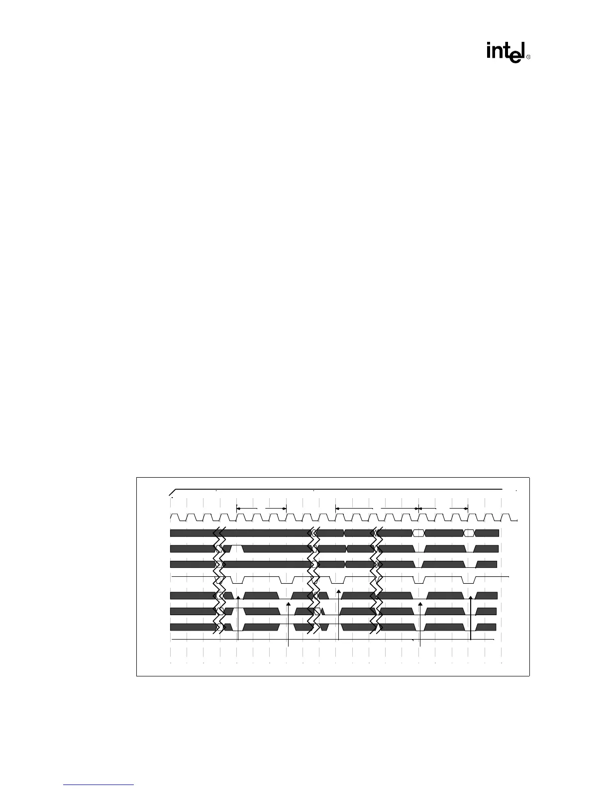
Initialization Sequence
The initialization sequence can be issued at anytime. Following the initialization sequence, the
device must be ready for full functionality. SGRAM devices are initialized by the following
sequence:
•
At least one NOP cycle will be issued after the 1msec device deselect.
•
A minimum pause of 200usec will be provided after the NOP.
•
A precharge all (PALL) will be issued to the SGRAM.
•
8 Auto refresh (CBR) refresh cycles will be provided.
•
A mode register set (MRS) cycle will be issued to program the SGRAM parameters
(e.g., Burst length, CAS# latency, etc.).
•
After MRS, the device should be ready for full functionality within 3 clocks after T
mrd
is met.
Figure 3. Power Up Initialization Sequence
TrpTrp TrcTrc TmrdTmrd
1st. Auto Refresh
(CBR)
Inputs Stable
for 200 usec
Precharge
All Banks
8th. Auto Refresh
(CBR)
MRS Command Legal Command
CKE
CLK
A(7:0)
A8/A9
BA
CS#
RAS#
CAS#
WE#
DQM