3 Device AGP MotherBoard Design
3-12
Intel740™ Graphics Accelerator Design Guide
3.2.2 Board Description
For a single Pentium II / Intel 440BX AGPset /Intel 740 Graphics Accelerator motherboard design,
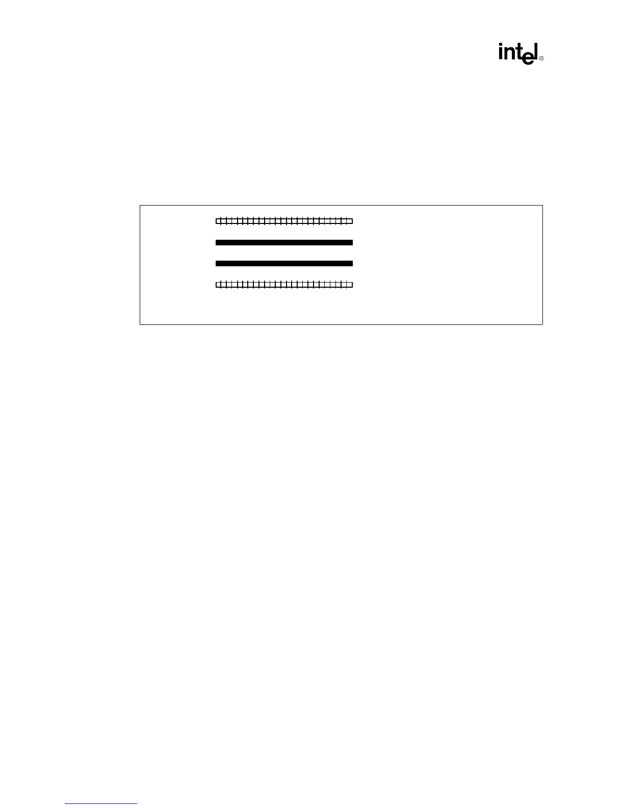
a 4 layer stack-up arrangement is recommended. The stack up of the board is shown in Figure 3-9.
The impedance of all the signal layers are to be 65 Ω ±15%. Lower trace impedance reduces signal
edge rates, overshoot & undershoot, and have less cross-talk than a higher trace impedance. A
higher trace impedance increases edge rates and may slightly decrease signal flight times.
Note that the top and bottom routing layers specify 1/2 oz. cu. However, by the time the board is
plated, the traces will end up about 1 oz. cu. Check with your fabrication vendor on the exact trace
impedance and PCB signal velocity value and insure that any signal simulation accounts for this.
Note: A thicker core may help reduce board warpage issues.
Additional guidelines on board buildup, placement and layout include:
•
For a 4-layer single processor design, double ended termination is recommended for GTL+
signals. One termination resistor is present on the Pentium II processor, and the other
termination resistor is needed on the motherboard. It may be possible to use single-ended
termination, if the trace lengths can be tightly controlled to a 1.5” minimum and 4.0”
maximum.
•
The termination resistors on the GTL+ bus should be 56 ohms ±5%.
•
The board impedance (Z) should be 65 ohms ± 15%.
•
FR-4 material should be used for the board fabrication.
•
The ground plane should not be split on the ground plane layer. If a signal must be routed for a
short distance on a power plane, then it should be routed on a VCC plane, not the ground
plane.
•
Keep vias for decoupling capacitors as close to the capacitor pads as possible.
3.2.3 3-point AGP Design Guidelines
3.2.3.1 Layout and Routing
With signal quality, timing, and clock issues in mind, a suitable bus layout and routing must be
found. Careful simulation as described in the Sensitivity Analysis section of this document is
essential. The nature of the logical point-to-point bus makes it a much harder topology to
implement than a physical point-to-point bus. The following discussion will focus on some layout
and routing issues associated with a logical point-to-point bus. The layout and routing for a logical
point-to-point bus is determined either from simulation results or are verified from simulation
Figure 3-9. Four Layer Board Stack-up
Primary Signal Layer (1/2 oz. cu.)
Ground Plane (1 oz. cu.)
Power Plane (1 oz. cu)
Secondary Signal Layer (1/2 oz. cu)
5 mils
47 mils
5 mils
PREPREG
CORE
PREPREG
Z = 60 ohms
Z = 60 ohms
Total board thickness = 62.6