3 Device AGP MotherBoard Design
3-10
Intel740™ Graphics Accelerator Design Guide
•
Timing Analysis
•
82443BX Memory Subsystem Layout and Routing Guidelines
— 100/66 MHz 82443BX Memory Array Considerations
— 3 DIMM Memory Layout & Routing Considerations
— PCI BUS Routing Guidelines
— Decoupling Guidelines for an Intel 440BX AGPset Platform
— Intel 440BX AGPset Clock Layout Recommendations
•
Design Checklist
•
Debug Recommendations
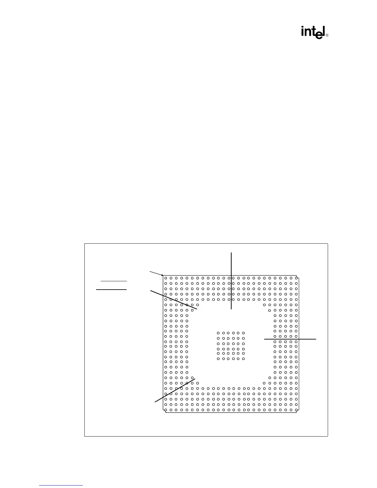
3.2.1 BGA Quadrant Assignment
The ball connections on the Intel740™ graphics accelerator have been assigned to simplify routing
and keep board fabrication costs down by enabling a 4-layer design. Figure 3-7 shows the four
signal quadrants of the Intel740 graphics accelerator. Component placement should be done with
this general flow in mind. This will simplify routing and minimize the number of signals which
must cross. The individual signals within the respective groups have also been optimized to be
routed using only 2 PCB layers.
A complete list of signals and ball assignments can be found in the Intel740™ Graphics
Accelerator Datasheet.
Figure 3-7. Major Signal Sections
Intel740
Top View
Pin #1 Corner
1 2 3 4 5 6 7 8 9 10 11 12 13 14 15 16 17 18 19 20 21 22 23
A
B
C
D
E
F
G
H
J
K
L
M
N
P
R
T
U
V
W
Y
AA
AB
AC
AD
AE
AF
A.G.P.
Quadrant
BIOS/Flicker
Quadrant
VMI Port
Quadrant
Local Memory
Quadrant