Intel740™ Graphics Accelerator Design Guide
2-21
Addin Card Design
2.3 Addin Card Schematics
This section describes the Intel740™ Graphics Accelerator Reference Design Schematics. Please
read this section carefully to observe all design recommendations and requirements.
The description of each schematic page is named by the logic block shown on that page.
Cover Sheet (Schematic Page 1)
The Cover Sheet shows the schematic page titles, page numbers, disclaimers and power pins.
Block Diagram (Schematic Page 2)
This page shows a block diagram overview of the Intel740 AGP card design. Schematic page
numbers for each of the major schematic components are shown.
Intel740™ Graphics Accelerator (Schematic Pages 3,4)
This page shows all of the connections to the Intel740 graphics accelerator. Each Intel740 graphics
accelerator interface is hooked up in this reference design. Beginning in the upper left hand corner
of the page, the video capture port is shown. Internally, the input pins are pulled down. These pins
contain a strapping option for subsystem ID. In this case the reference design has an ID of 0100h.
Bits that should be a “1” may be pulled up using a 2K pull-up resistor. If the graphics design will
not have video, the only concern is pulling the bus up to the correct value for the subsystem ID.
The video control signals may be left unconnected. The BIOS interface multiplexes the BIOS,
vendor ID, and flicker filter TV encoder. The ROMA lines are internally pulled down and may be
pulled up using a 2K pull-up resistor. The video host port connects directly to the VMI header. The
section labeled AGP interface connects directly to the AGP connector. The memory interfaces
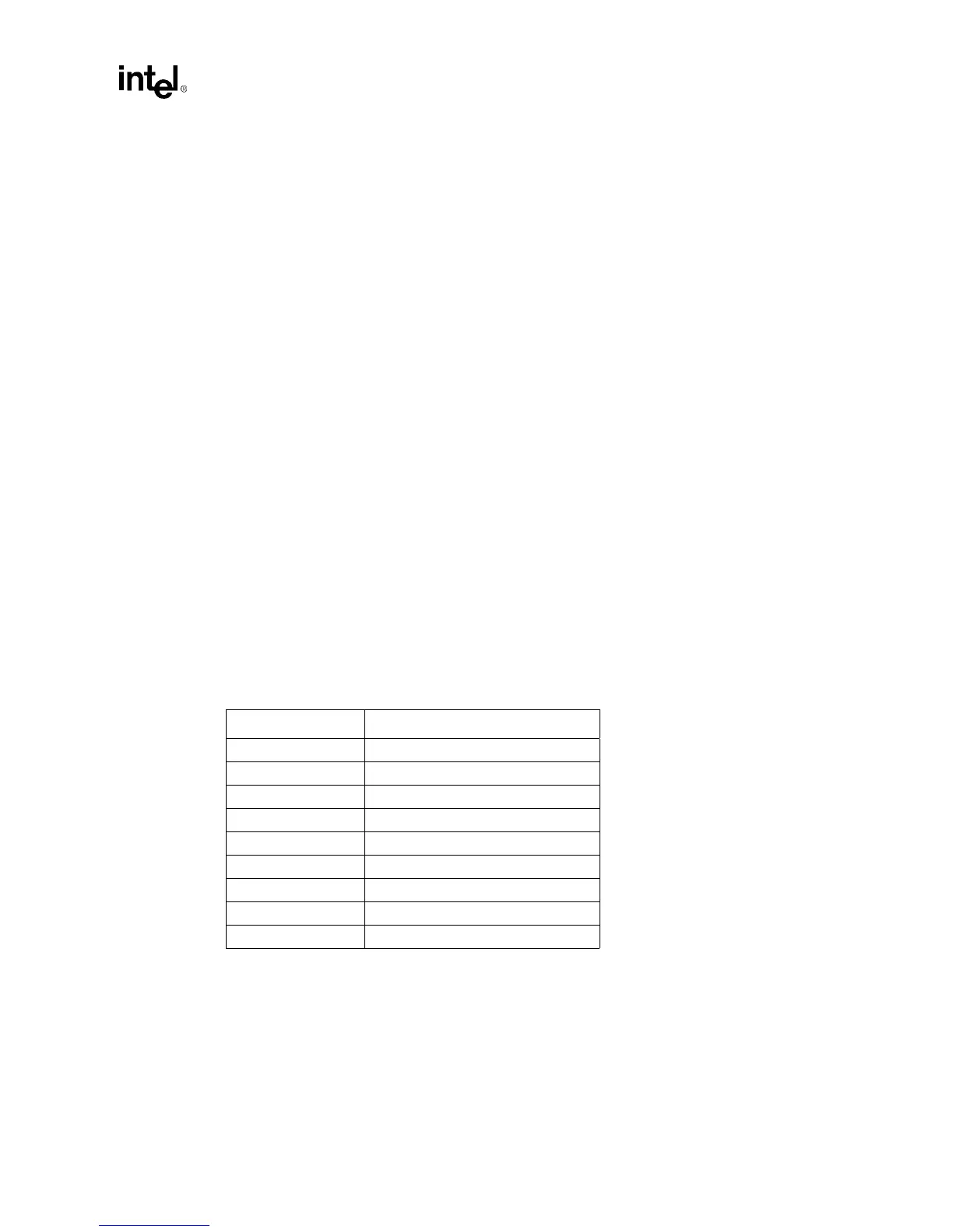
connect to an SO-DIMM connector and memory components. Each of the 9 GPIOs serve a
different function in the reference design. Table 2-13 lists the function assigned to the GPIOs.
Decoupling for the Intel740 graphics accelerator is shown along the bottom of the schematic page.
Table 2-13. GPIO Functions
GPIO FUNCTION
GPIO0 I
2
C Data
GPIO1 I
2
C Clock
GPIO2 DDC Data
GPIO3 DDC Clock
GPIO4 Fan Fail
GPIO5 Extra For DVD Control
GPIO6 VP[15:0] Bus Isolation Control
GPIO7 Extra For DVD Control
GPIO8 Power Down