SO-DIMM Module — Unbuffered SDRAM/SGRAM Graphics
12
Revision 0.91
7.0 Electrical Characteristics
The module electrical characteristics are carefully controlled to allow system configurations with
two separate memory arrays. This allows one module to be present, plus memory soldered directly
to the motherboard or add-in card PCB. Currently, two modules are not being supported. Routing
on the main board will generally be done as a T-topology. The module’s electrical characteristics
(as well as the main board’s characteristics) must be carefully implemented to insure a balanced
T-topology.
The board must have a characteristic impedance between 50 and 85 ohms.
The following table lists the suggested flight time budgets for a typical graphic system using an
early/late memory clock.
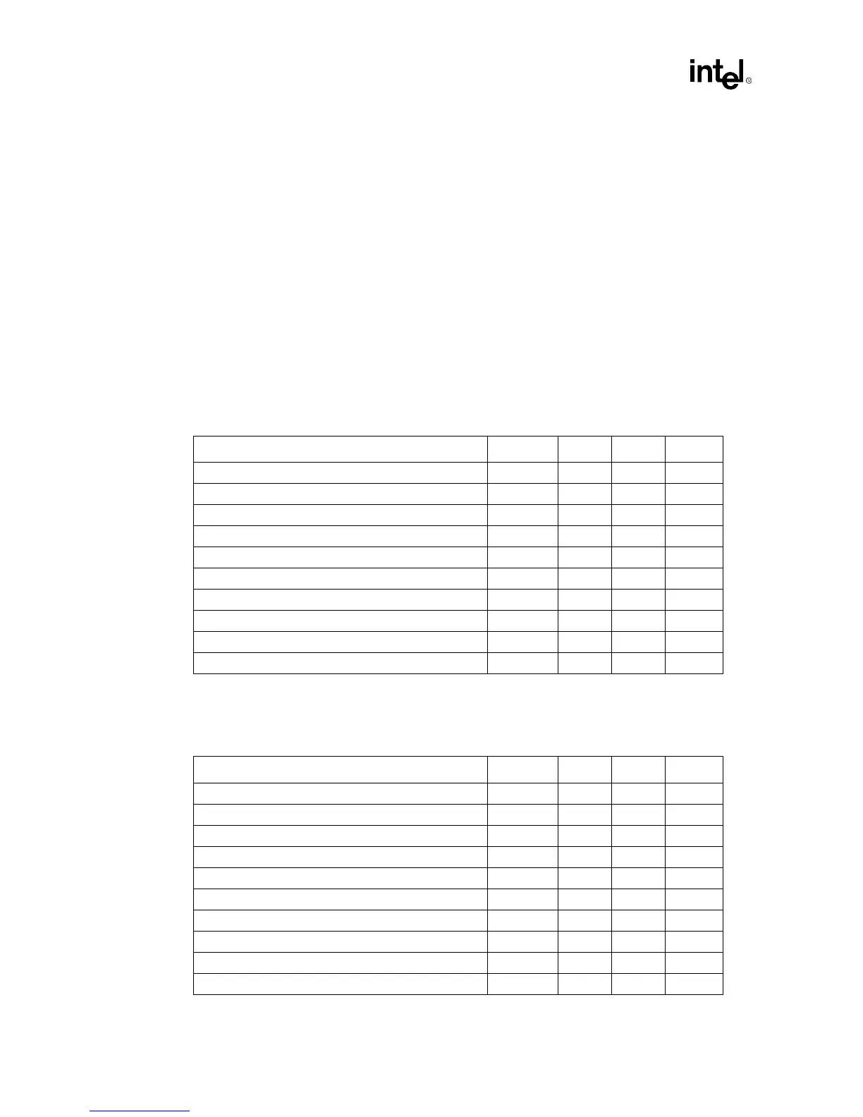
7.1 15 nS Timing
7.2 12 nS Timing
Parameter Symbol Min. Max. Unit
Clock Cycle Time Tcyc 15.0 nS
Early/Late Clock Tcsk 0.35 1.6 nS
Output Valid from Clock Tac 11.0 nS
Output Hold from Clock Toh 2.5 nS
Input Setup Time Tsi 3.0 nS
Input Hold Time Thi 1.0 nS
Motherboard Clock Flight Time Tcfm 0 0.3 nS
Motherboard Addr/Data/Cntrl Flight Time Txfm 0 0.3 nS
Module Clock Flight Time Tcfs 0.1 0.365 nS
Module Flight Addr/Data/Cntrl Flight Time Txfs 0 0.375 nS
Parameter Symbol Min. Max. Unit
Clock Cycle Time Tcyc 12.0 nS
Early/Late Clock Tcsk 1.3 1.8 nS
Output Valid from Clock Tac 9.0 nS
Output Hold from Clock Toh 2.5 nS
Input Setup Time Tsi 3.0 nS
Input Hold Time Thi 1.0 nS
Motherboard Clock Flight Time Tcfm 0.2 0.3 nS
Motherboard Addr/Data/Cntrl Flight Time Txfm 0 0.3 nS
Module Clock Flight Time Tcfs 0.175 0.325 nS
Module Flight Addr/Data/Cntrl Flight Time Txfs 0 0.375 nS