Intel740™ Graphics Accelerator Design Guide
2-5
Addin Card Design
2.2 Layout and Routing Guidelines
This chapter describes layout and routing recommendations to insure a robust design. These
guidelines should be followed as closely as possible. Any deviations from the guidelines listed here
should be simulated to insure adequate margin is still maintained in the design.
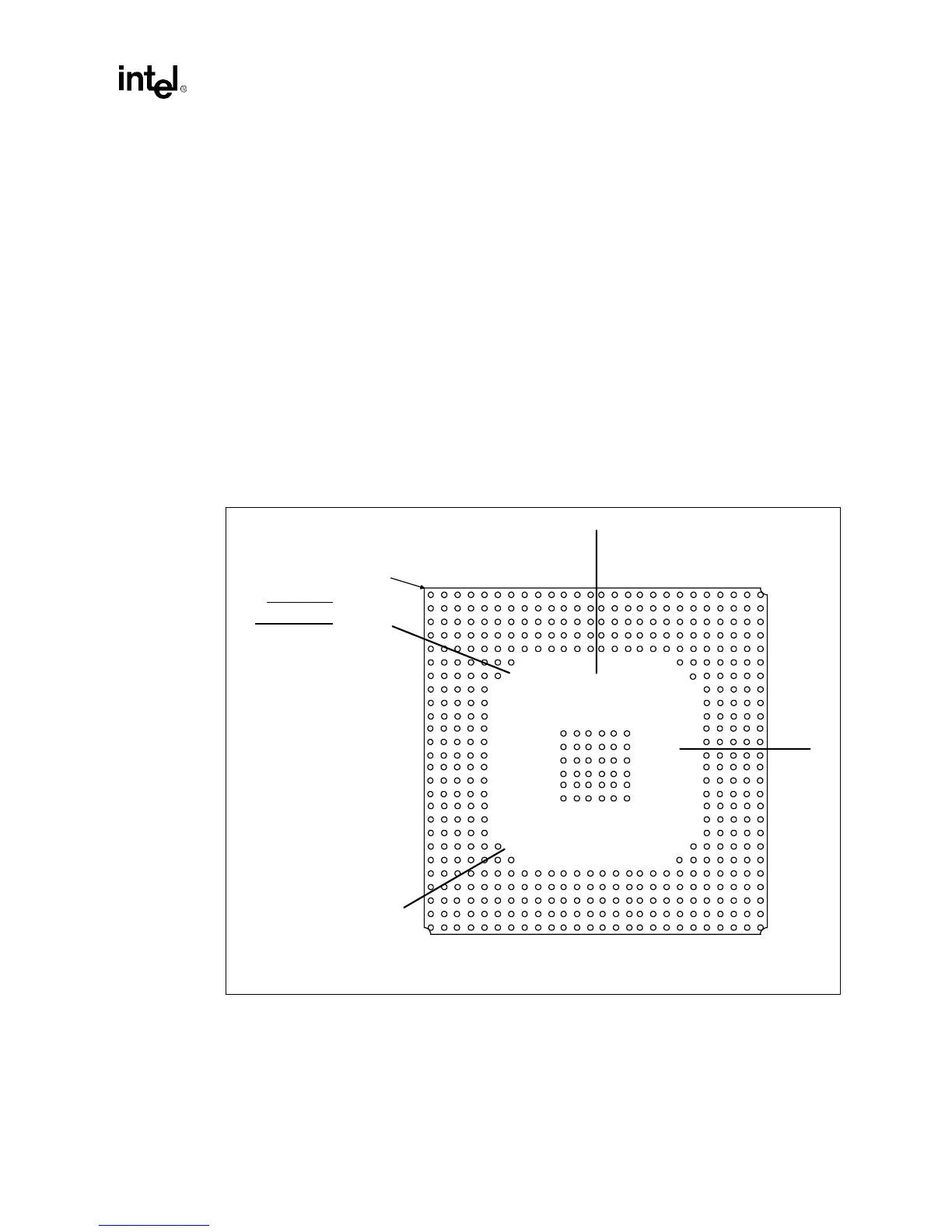
2.2.1 Placement
The ball connections on the Intel740™ graphics accelerator have been assigned to simplify routing
and keep board fabrication costs down by enabling a 4-layer design. Figure 2-3 shows the four
signal quadrants of the Intel740 graphics accelerator. Component placement should be done with
this general flow in mind. This will simplify routing and minimize the number of signals which
must cross. The individual signals within the respective groups have also been optimized to be
routed using only 2 PCB layers.
A complete list of signals and ball assignments can be found in the Intel740™ Graphics
Accelerator Datasheet.
Figure 2-3. Major Signal Sections
Intel740
Top View
Pin #1 Corner
1 2 3 4 5 6 7 8 9 10 11 12 13 14 15 16 17 18 19 20 21 22 23
A
B
C
D
E
F
G
H
J
K
L
M
N
P
R
T
U
V
W
Y
AA
AB
AC
AD
AE
AF
A.G.P.
Quadrant
BIOS/Flicker
Quadrant
VMI Port
Quadrant
Local Memory
Quadrant