Intel740™ Graphics Accelerator Design Guide
2-13
Addin Card Design
2.2.6.2 Power Planes
The Bt869 and associated circuitry have two power planes, VCC3 and 3VAA_BT869. The
3VAA_BT869 plane is a separate cutout, joined to VCC3 by a ferrite bead. The device should
reside entirely above the 3VAA_BT869 plane, as there are no VCC3 connections to the device. So
long as the 3VAA_BT869 plane underlies all the analog components, it should be as small as
possible.
2.2.6.3 Passive Components and Signal Routing
All passive components should be placed as close to the Bt869 device as possible. These devices
consist of: the 0.1µF and 0.01µF bypass capacitors, the 10µF capacitors, the crystal oscillator
circuitry, and the 0.1µF capacitors and 75 ohm resistors at the VREF, VBIAS and FSADJUST pins
as well as the protection diodes.
Note: There must be NO digital signals routed under or above the analog power and ground planes
(3VAA_BT869 and AGND).
The filter circuits on the three video output signals (TVOUT_Y, TVOUT_C, TVOUT_CVBS)
must be very near the 50-pin connector or other output connectors. Long lengths of closely spaced
parallel analog signals should be avoided. Wherever analog signals run in parallel, separated by
less than 15 mils for longer than 250 mils, run a ground line between the video input traces of
approximately 12 mils width.
2.2.6.4 AGP Layout and Routing Guidelines
This section describes the group of signals that runs between the Intel740 graphics accelerator
AGP Interface and the AGP edge connector. For the definition of AGP functionality (protocols,
rules and signaling mechanisms, as well as the platform level aspects of AGP functionality), refer
to the latest AGP Interface Specification. This document focuses only on specific Intel740 graphics
accelerator recommendations for the AGP interface. The general length requirements are shown in
Table 2-6.
Mismatch between strobe and data traces must be less than 0.5”. Thus the trace length for signals
within a group must be within ±0.5” of the corresponding strobe’s trace length, as indicated in
Table 2-7.
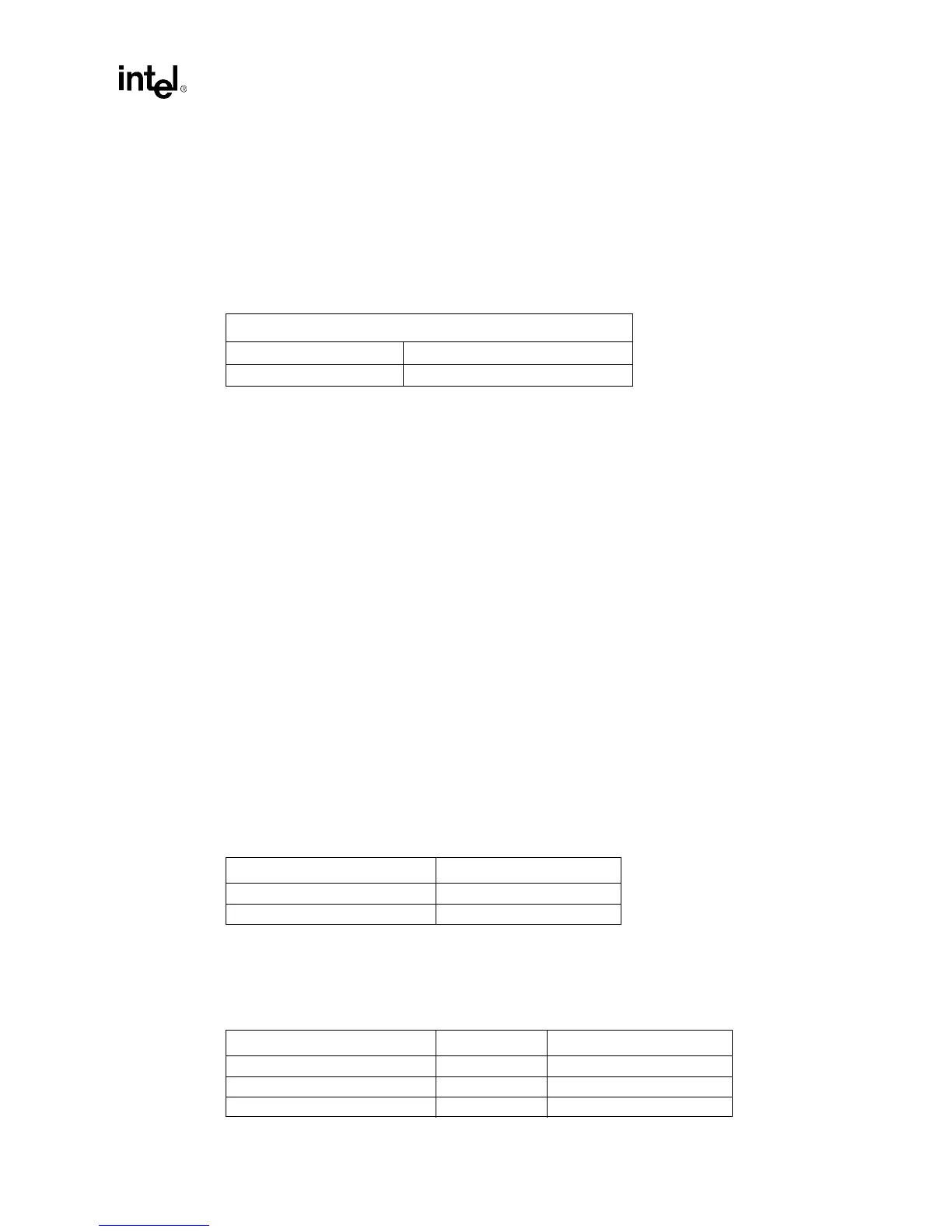
Table 2-5. Bt869 Digital and Analog Power Pins
Bt869 3V Pins
3VAA_BT869 (Analog) 69, 71, 73, 80
3VAA_BT869 (Digital) 19, 20, 30, 40, 46, 47, 57, 60, 61
Table 2-6. AGP Signal Lengths
Group Recommendation
All
≤
3.0”
CLK 2.6” ± 0.4”
Table 2-7. Strobes and Corresponding Signal Groups
Group Strobe Recommendation
AD[31:16], C/BE[3:2]# AD_STB_B L
AD_STB_B
± 0.5”
AD[15:0], C/BE[1:0]# AD_STB_A L
AD_STB_A
± 0.5”
SBA[7:0] SB_STB L
SB_STB
± 0.5”