SO-DIMM Module — Unbuffered SDRAM/SGRAM Graphics
16
Revision 0.91
8.0 PCB Layout Considerations
To insure proper signal integrity, the module routing must be taken under careful considerations.
This section outlines PCB layout considerations for the SO-DIMM module.
Each section looks at three separate topologies; one for clocks, one for control/address, and one for
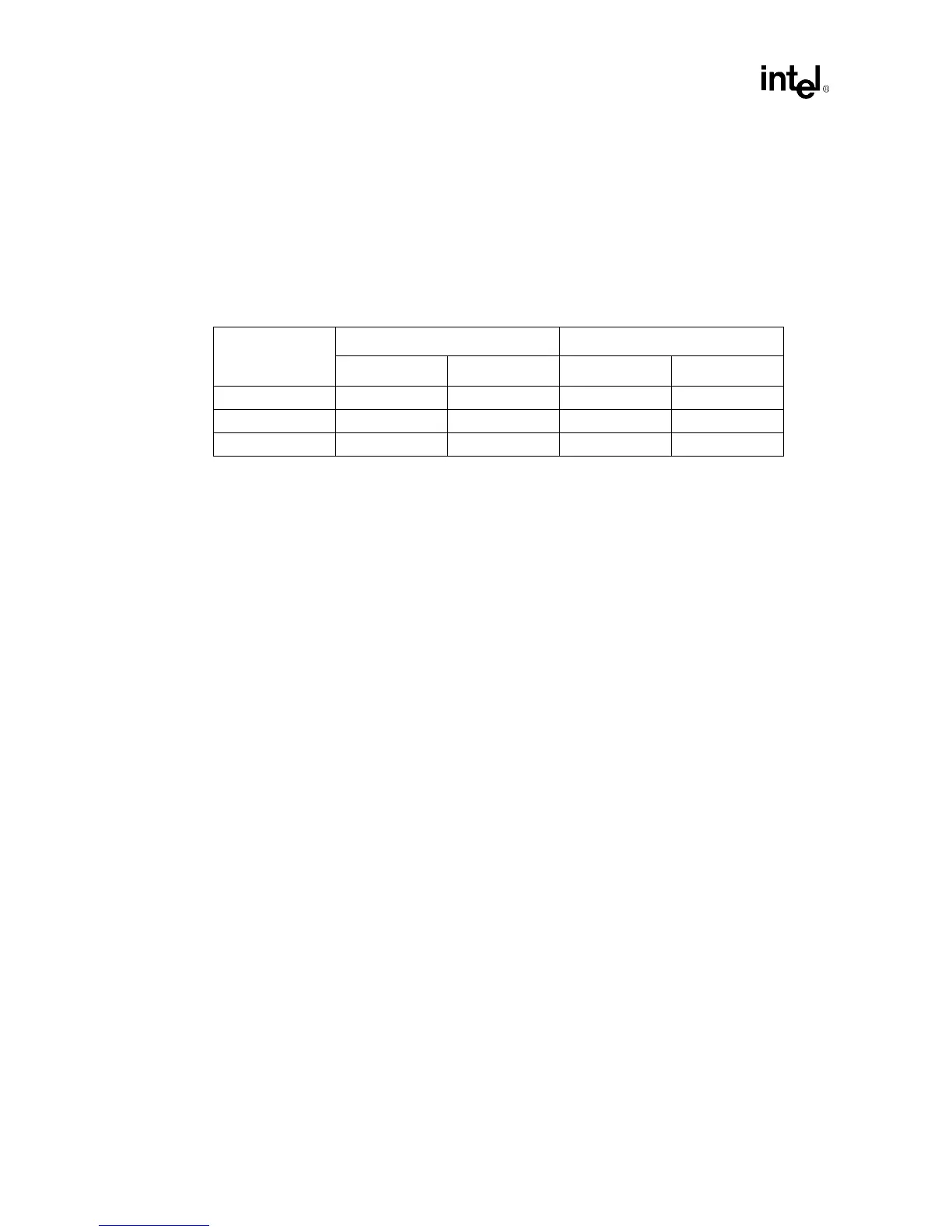
data. The assumed loading for this configuration is:
Table 5. Signal Loading
Signal 32-bit 64-bit
Single-sided Double-sided Single-sided Double-sided
clocks 1 load 1 load 2 loads 2 loads
address/control 1 load 2 loads 2 loads 4 loads
data 1 load 2 loads 1 load 2 loads