Revision 0.9
23
PC SGRAM Specification
9.4 DC Specifications for 166-250 MHz
Absolute Maximum D.C. Rating (TBD)
D.C Operating Requirements (TBD)
9.5 A.C. Specifications for 166-250 MHz
Maximum AC Operating Requirements (TBD)
Refresh Rate (TBD)
9.6 A.C. Timing Parameters for 166-250 MHz
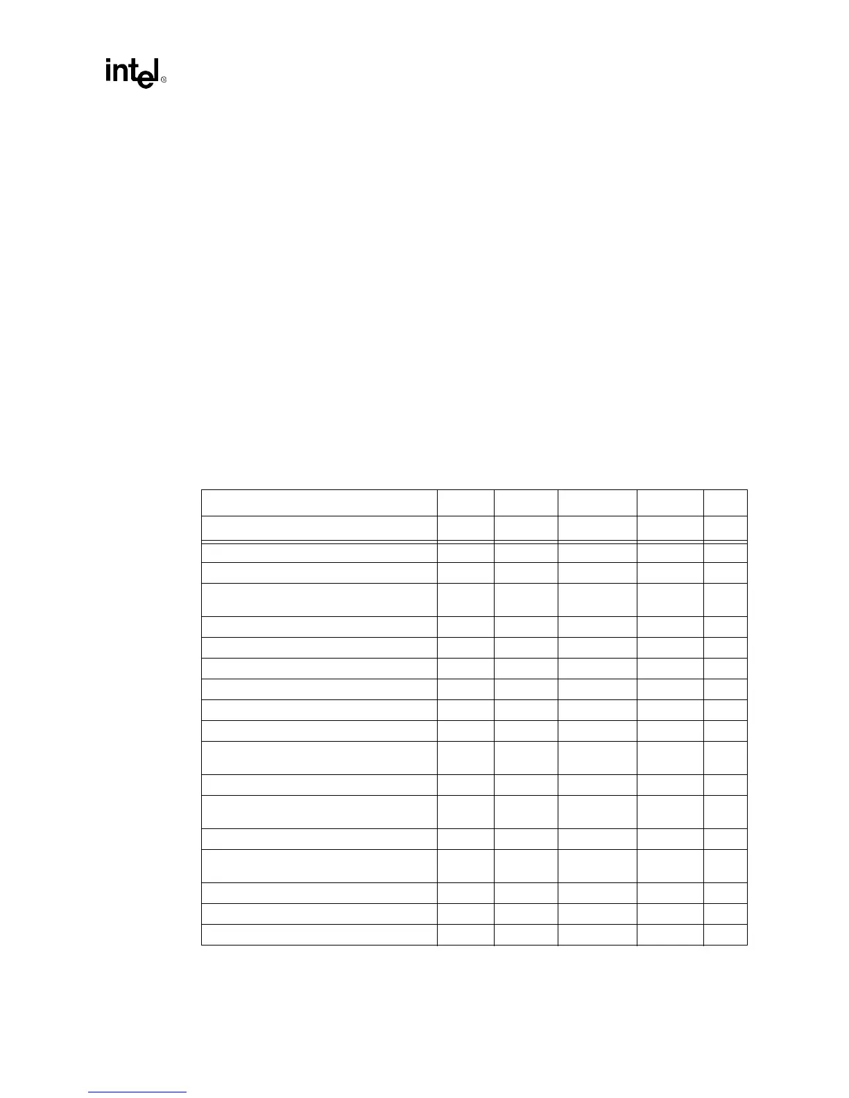
Table 14. 166, 200, 250 MHz & 166 MHz AC Timing Parameters
166 200 250
Parameter Symbol Min Max Min Max Min Max Units
Clock Period t
CK
65 4 ns
CAS Latency CL 2 3 2 3 2 3 CLK
CLK to valid output delay (max)
T
AC
(max)
5.5 TBD TBD ns
Output data hold time T
OH
2.5 TBD TBD ns
Address & Command Input setup time T
AS
1TBDTBDns
Address & Command Input hold time T
AH
1TBDTBDns
Data Input setup time T
DS
1TBDTBDns
Data Input hold time T
DH
1TBDTBDns
Activate to Activate Delay (Different bank) T
RRD
2 TBD TBD CLK
Read to Read Command Delay,Write to Write
Command Delay
T
CCD
2 TBD TBD CLK
Activate to Read, Write or Block Write Delay T
RCD
3 TBD TBD CLK
Precharge to Activate Delay (single bank
precharge)
T
RP
3 TBD TBD CLK
Activate to Precharge Delay T
RAS
7 TBD TBD CLK
Activat to Activate Delay (Same Bank),
Refresh Cycle time
T
RC
11 TBD TBD CLK
Block Write to Precharge Delay T
BPL
2 TBD TBD CLK
Block Write Cycle Time T
BWC
2 TBD TBD CLK
Last write data in to precharge T
DPL
2 TBD TBD CLK