Addin Card Design
2-16
Intel740™ Graphics Accelerator Design Guide
Figure 2-15. Layout Dimensions (WEB#, SRASB#, SCASB#, CSA0#)
Table 2-11. Memory Layout Restrictions (See Figure 2-16 and Figure 2-17)
Signal
Intel740™ to
Resistor
Resistor to
SO-DIMM
SO-DIMM to
SGRAM Stub
SGRAM Stub
Min Max
TCLK0 0.6” 2.4” ±0.25” n/a n/a n/a
TCLK1 0.6” 2.4” ±0.25” 1.0” 0.4” 0.6”
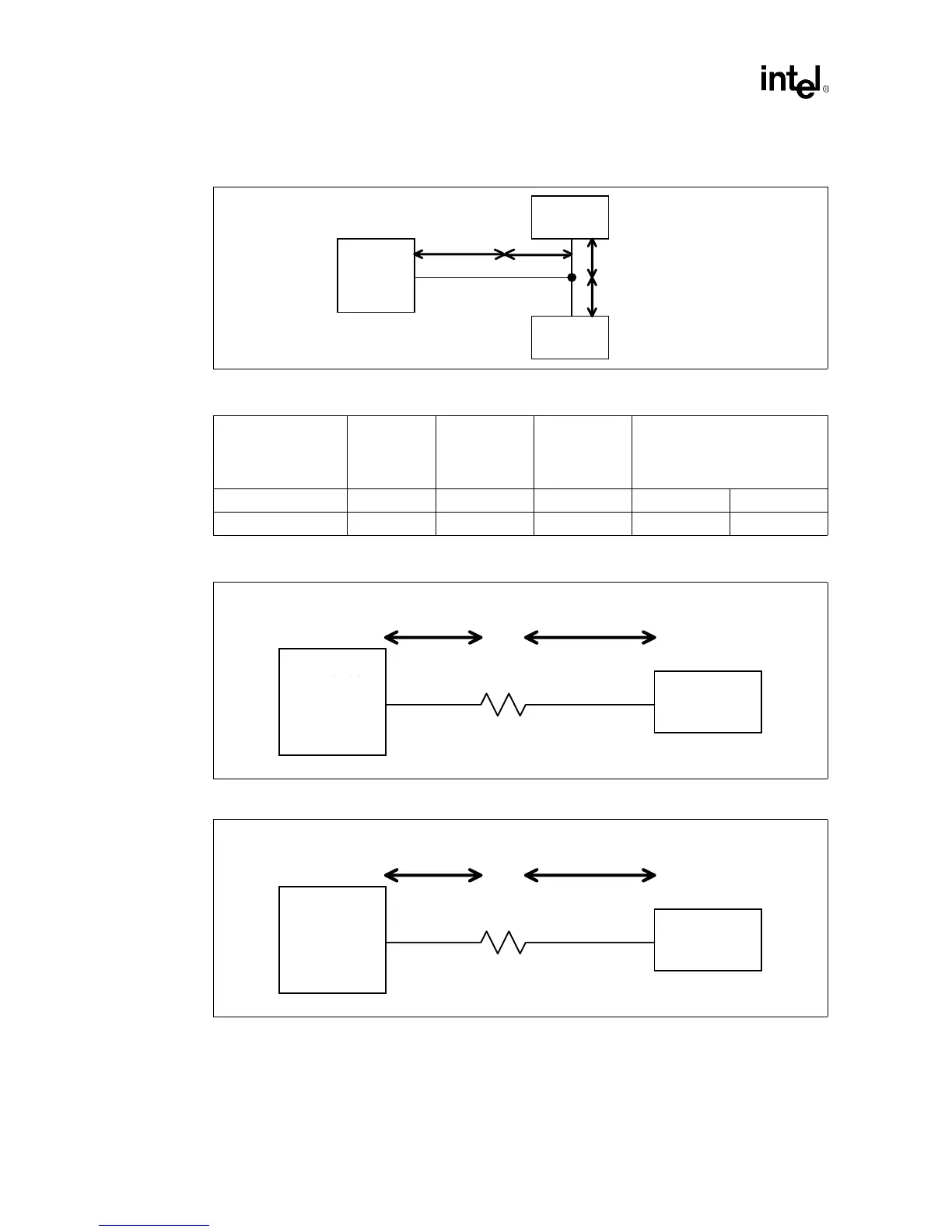
Figure 2-16. Memory Layout Dimensions (TCLK0)
Figure 2-17. Memory Layout Dimensions (TCLK1)
Intel740
2.0” - 4.0”
SGRAM
SGRAM
0.25” - 0.6”
0.25” - 0.6”
0.25” - 0.9”
Intel740
™
Chip
Intel740
SO-DIMM
Connector
0
Ω
2.4” +/- 0.25”
0.6”
Intel740™
Chip
Intel740
SO-DIMM
Connector
0
Ω
2.4” +/- 0.25”
0.6”
Intel740™
Chip