Intel740™ Graphics Accelerator Design Guide
2-17
Addin Card Design
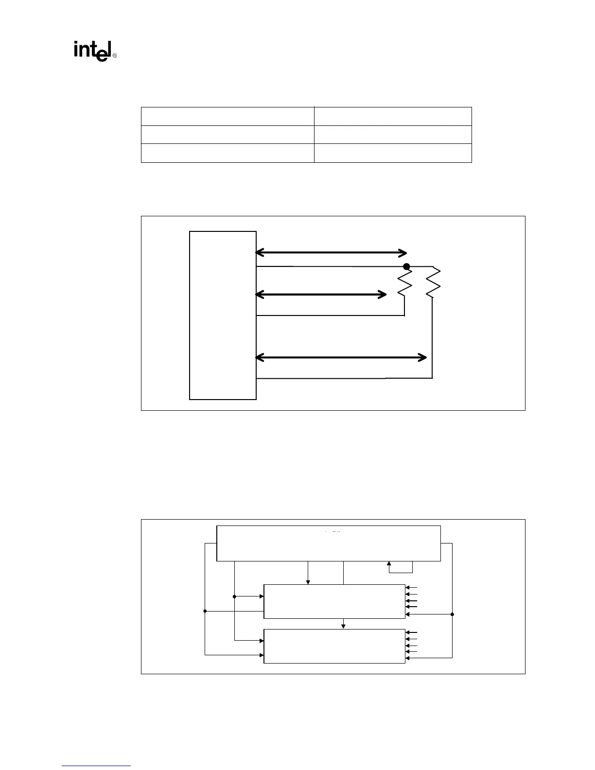
Note: It is important to match clock lengths. For example, if the length from OCLK to Resistor is 1.03,
then the length from Resistor to RCLK should be 3.03.
2.2.6.6 Intel740™ Graphics Accelerator Memory Configurations
In the following discussion the term row refers to a set of memory devices that are simultaneously
selected by an SRAS and the CS# signal.
Configuration #1: In this configuration, the minimum amount of memory (2MB) is supported.
Note that, the same copy of all control signals goes to each component.
Signal Intel740™ to Resistor
OCLK to Resistor 2.75” ±0.25
RCLK0, RCLK1 3.0” ±0.25”
Figure 2-18. Memory Layout Dimensions (RCLK and OCLK to RCLK)
Intel740
33
Ω
33
Ω
2.75” +/- 0.25
OCLK
RCLK0
RCLK1
3.0” +/- 0.25”
3.0” +/- 0.25”
Intel740™
Chip
Figure 2-19. 2/4 MB Local Memory Connection (64-bit data path)
Intel740
MD[63:0]
CSx[A:B]# DQM[3:0] DQM[7:4] RCLKx OCLK
MA[11:0]
WEA#
SRASA#
SCASA#
TCLKA
WEA#
SRASA#
SCASA#
TCLKA
256K/512K X 32
256K/512K X 32
CS0A#
CS0A#
MD[31:0]
MD[63:32]
Intel740™ Chip