Addin Card Design
2-20
Intel740™ Graphics Accelerator Design Guide
2.2.6.7 TV Out Interface
The TV out bus is the group of signals that carry digitized display data from the Intel740
graphics accelerator to the Bt869 flicker filter TV-out component. This interface is shared with
the BIOS interface. Table 2-12 gives the maximum trace lengths between components.
2.2.6.8 Analog Signals
It is recommended that all analog signal traces be 75Ω ±5%. It is important that these traces not
violate the 5x10 mil spacing for the 65Ω traces. Analog traces include the DAC R, G, B traces, all
of the inputs to the Bt829B component and outputs from the Bt869 component.
2.2.7 UL and FCC Considerations
Certain precautions should be taken in the design of the of a graphics card to ensure passing safety
and EMI tests. These precautions are listed below.
•
When a signal can be hot plugged, clamping diodes should be used to limit voltage spikes.
•
When a voltage leaves the card, a fuse should be placed in the path to protect from a short
circuit.
•
Sockets, Fans and Brackets should be grounded.
•
Separate Power Planes of the same voltage should be stitched together.
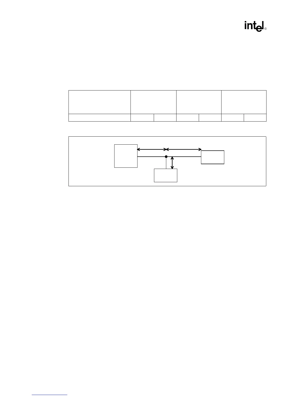
Table 2-12. TV Out/ROMA Trace Lengths (See Figure 2-22)
Signal
Intel740™ to BIOS
Stub
BIOS Stub BIOS to Bt869
Min Max Min Max Min Max
ROMA[17:0] 0.0” 3.5” 0.0” 1.5” 0.0” 4.0”
Figure 2-22. Layout Dimensions, Digital TV Bus
Intel740
0.0” - 3.5”
BIOS ROM
0.0” - 4.0”
0.0” - 1.5”
Bt869
Intel740™
Chip