Revision 0.91
21
SO-DIMM Module — Unbuffered SDRAM/SGRAM Graphics
9.0 Electrical Specifications
The following information is from the Intel PC SDRAM Specification, version 1.1, April 1996. It is
provided here for convenience
9.1 SDRAM/SGRAM Component Absolute Maximum D.C.
Ratings
9.2 SDRAM/SGRAM Components D.C. Operating Requirements
NOTES:
1. Input leakage currents include hi-Z output leakage for all bi-directional buffers with tri-state outputs.
2. This is a recommendation, not an absolute requirement. The actual value should be provided with the
component data sheet.
9.3 SDRAM/SGRAM Components Absolute Maximum A.C.
Operating Requirements
NOTE: The overshoot and undershoot voltage duration is
≤
5ns with no input clamp diodes.
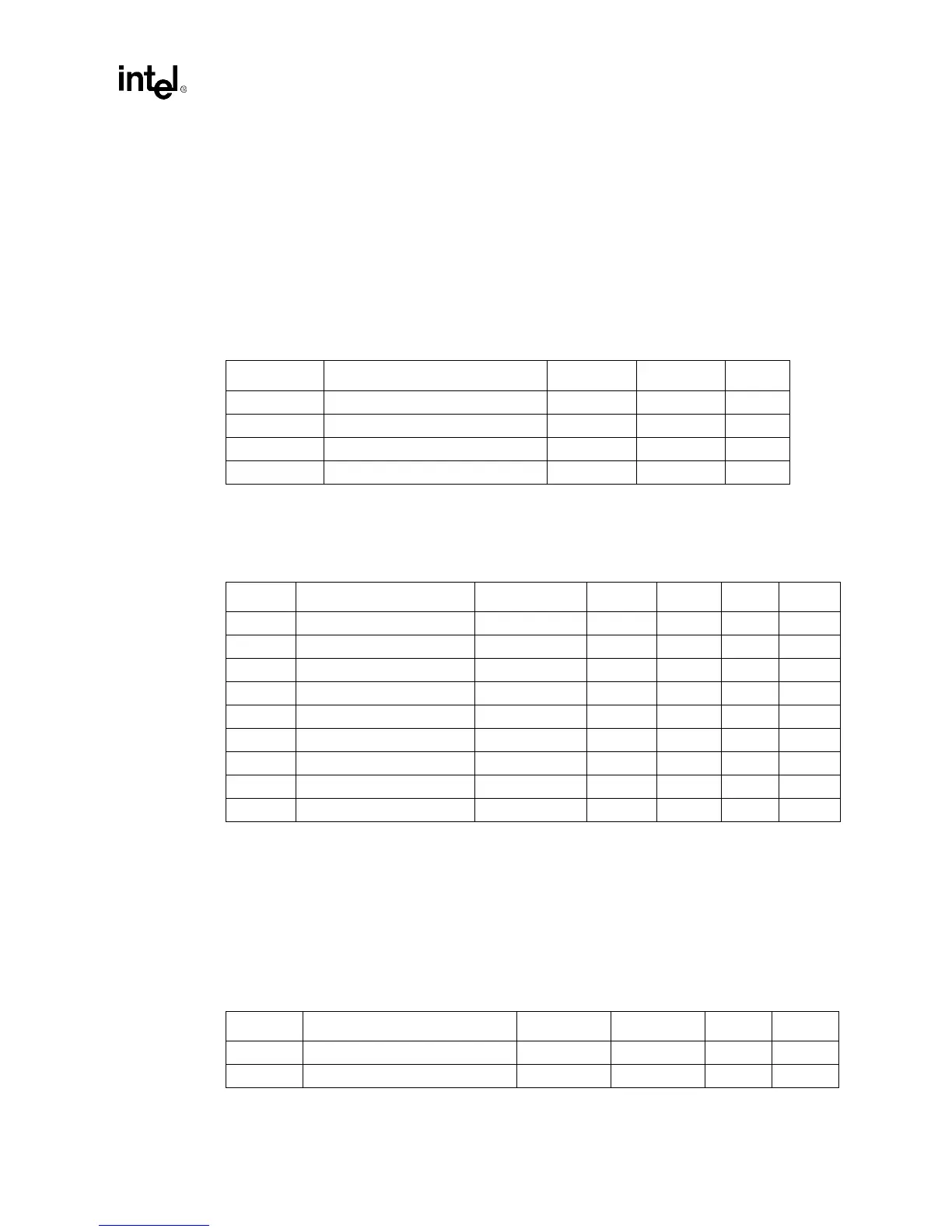
Table 10. Absolute Maximum Ratings
Symbol Parameter Min. Max. Units
Vin, Vout Voltage on any pin w.r.t V
SS
-0.5 VCC + 0.5 V
VCC, VCC
Q
Voltage Supply pins w.r.t V
SS
-0.5 4.5 V
Ts Storage Temperature -55 125
°
C
PD Power Dissipation 1 W
Table 11. D.C. Operating Requirements
Symbol Parameter Condition Min. Max. Units Notes
VCC Supply Voltage 3.0 3.6 V
VCCQ I/O Supply Voltage 3. 0 3.6 V
Iil Input Leakage Current 0 < Vin < VCCQ -5 +5
µ
A1,2
Voh Output High Voltage Ioh = -4 mA 2.4 V
Vol Output Low Voltage Iol = 4 mA 0.4 V
Cin Input/Clock Pin Capacitance 5 pF
CI/O I/O Pin Capacitance 7 pF
Lpin Pin Inductance 10 nH 2
Ta Ambient Temperature No Airflow 0 65
°
C
Table 12. Absolute Maximum A.C. Operating Requirements
Symbol Parameter Min. Max. Units Notes
Vih Input High Voltage 2.0 VCCQ + 1.5 V 1
Vil Input Low Voltage VSSQ
−
1.5 0.8 V 1