Intel740™ Graphics Accelerator Design Guide
3-5
3 Device AGP MotherBoard Design
3.1.4.3 GPO27# and GPO28# Signal Duration
NOTE:
1. 1ms is the smallest system BIOS increment of time
2. This is the propagation delay from when GPO28# is asserted to valid output at TEST.
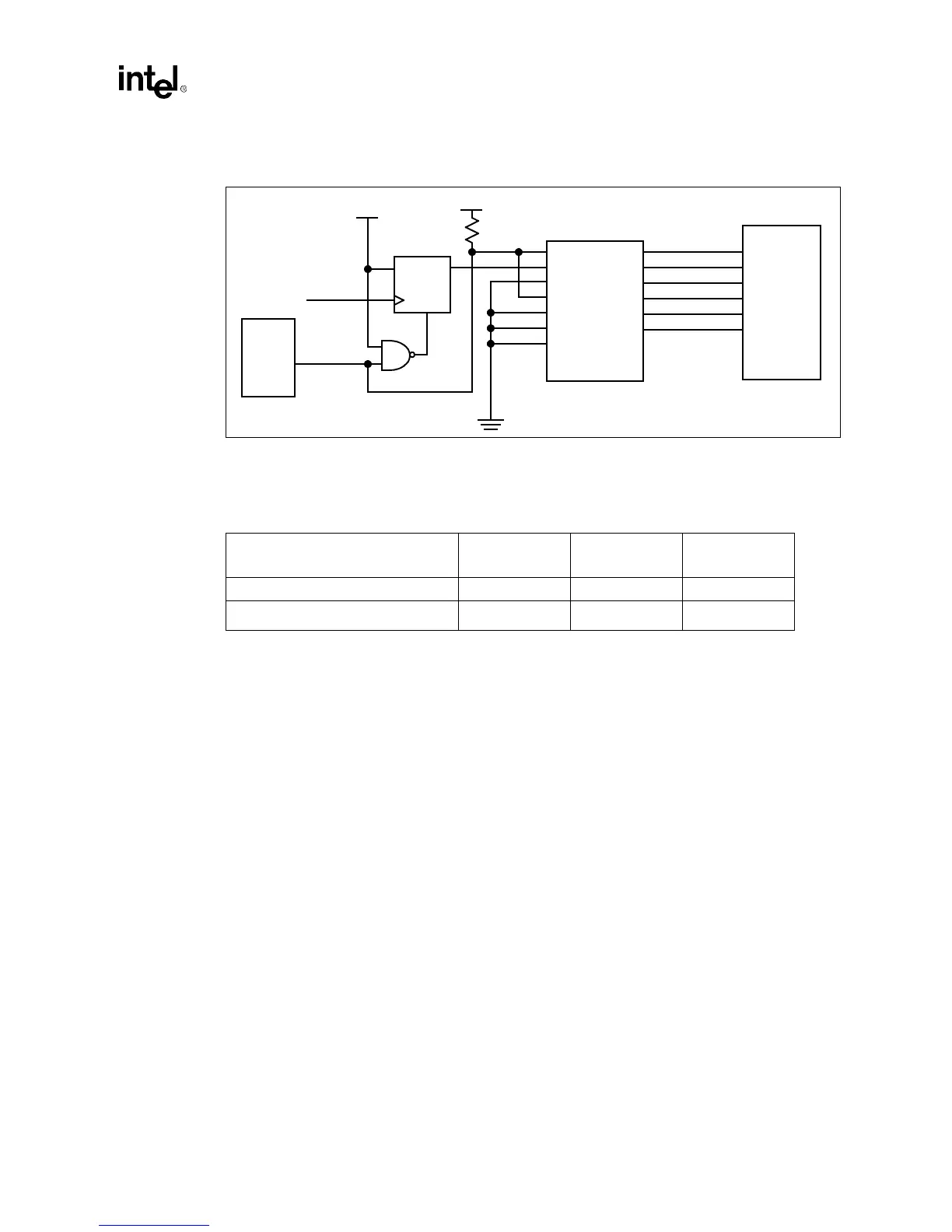
Controls Signals From the PIIX4
GPO27 takes the device out of low power mode and puts it into functional mode. The duration of
the GPO27 signal should be the minimum of 1ms (see Table 3-2). This requirement is set by the
minimum reset time defined in the Accelerated Graphics Port Interface Specification, Revision 1.0.
GPO28 puts the device into low power mode and should be a minimum duration of the sum of the
propagation delay for logic depicted in Figure 3-2.
Figure 3-3. The Schematic Diagram for the WEB#, SCASB#, SRASB#, CS0B#, CS1B# and TEST
Table 3-2. Signal Duration of the GPO Signals from PIIX4
Signal Active
Minimum
Duration
Actual Duration
1
GPO27 from PIIX4 Low (0) 1ms 1ms
GPO28 from PIIX4 Low (0) see note
2
1ms
PIIX4E
Vcc3
D
Q
CLR#
Intel740™
Chip
GPO28#
SYSCLK
OE#
IN1
IN2
IN3
IN4
IN5
IN6
OUT1
OUT2
OUT3
OUT4
OUT5
OUT6
Vcc3
TEST
WEB#
SCASB#
SRASB#
CS0B#
CS1B#
2.2 K
Ω