PC SGRAM Specification
22
Revision 0.9
NOTE:
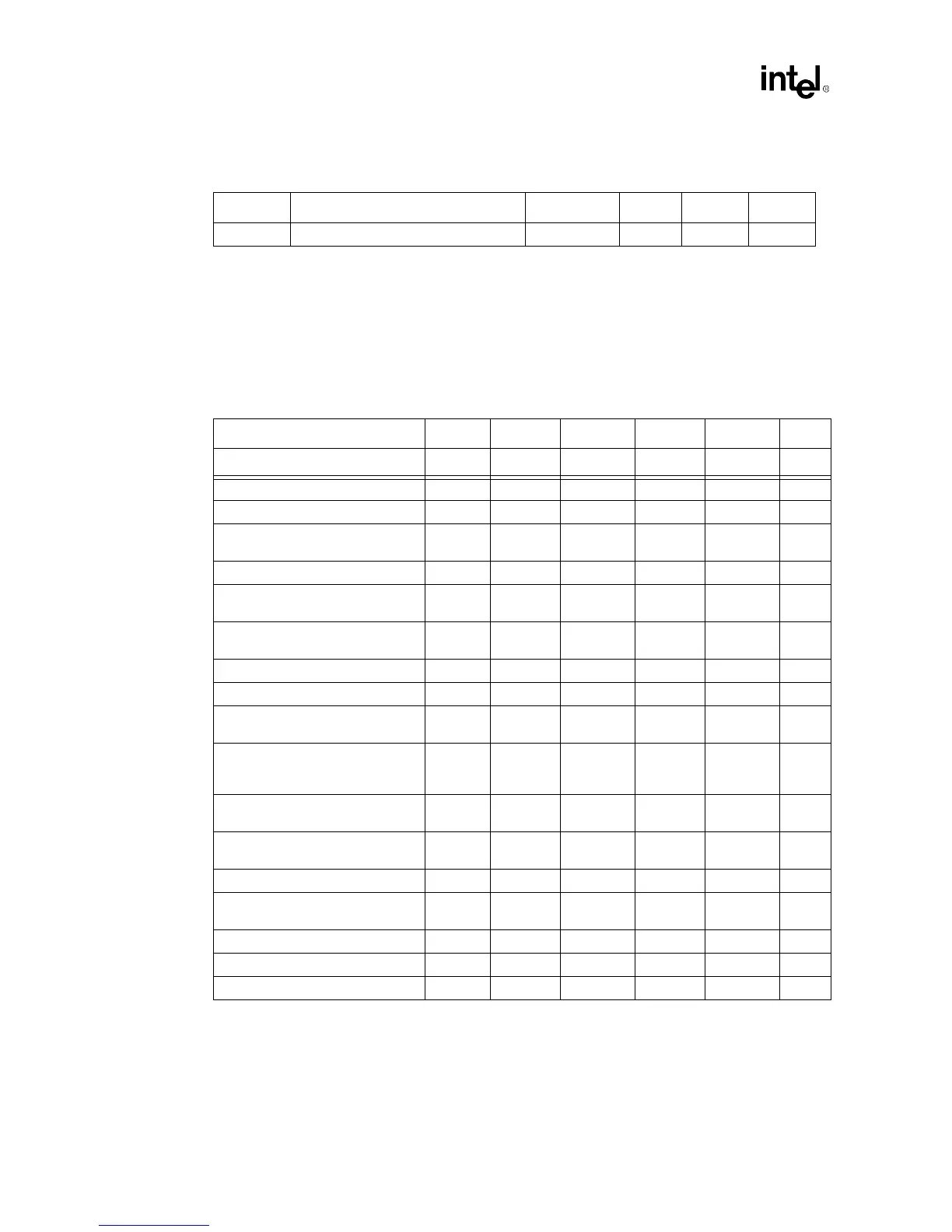
1. The overall array refresh is determined by multiplying the specified row refresh rate by the number of rows in
the total array.
9.3 A.C. Timing Parameters for 100-166 MHz
NOTE:
1. Output I/O Timings measured with a 30pf load
Table 12. Refresh Rate
Symbol Parameter Min Max Units Notes
Tref Refresh rate / row 15.6 usec 1
Table 13. 100, 125, 143MHz & 166MHz AC Timing Parameters
100
125 143 166
Parameter Symbol Min Max Min Max Min Max Min Max Units
Clock Period t
CK
10 8 7 6 ns
CAS Latency CL 2 3 2 3 2 3 2 3 CLK
CLK to valid output delay (max)
T
AC
(max)
7665.5ns
Output data hold time T
OH
2.5 2.5 2.5 2.5 ns
Address & Command Input setup
time
T
AS
2.5 2.5 2 1 ns
Address & Command Input hold
time
T
AH
11 11 ns
Data Input setup time T
DS
2.5 2 1.5 1 ns
Data Input hold time T
DH
11 11 ns
Activate to Activate Delay (Different
bank)
T
RRD
22 22 CLK
Read to Read Command
Delay,Write to Write Command
Delay
T
CCD
11 11 CLK
Activate to Read, Write or Block
Write Delay
T
RCD
23 33 CLK
Precharge to Activate Delay (single
bank precharge)
T
RP
23 33 CLK
Activate to Precharge Delay T
RAS
56 77 CLK
Activat to Activate Delay (Same
Bank), Refresh Cycle time
T
RC
7 9 10 11 CLK
Block Write to Precharge Delay T
BPL
22 22 CLK
Block Write Cycle Time T
BWC
22 22 CLK
Last write data in to precharge T
DPL
11 11 CLK