Addin Card Design
2-8
Intel740™ Graphics Accelerator Design Guide
2.2.3 BGA Component
2.2.3.1 Layout Requirements
The following layout requirements should be followed when routing the 468 MBGA package.
•
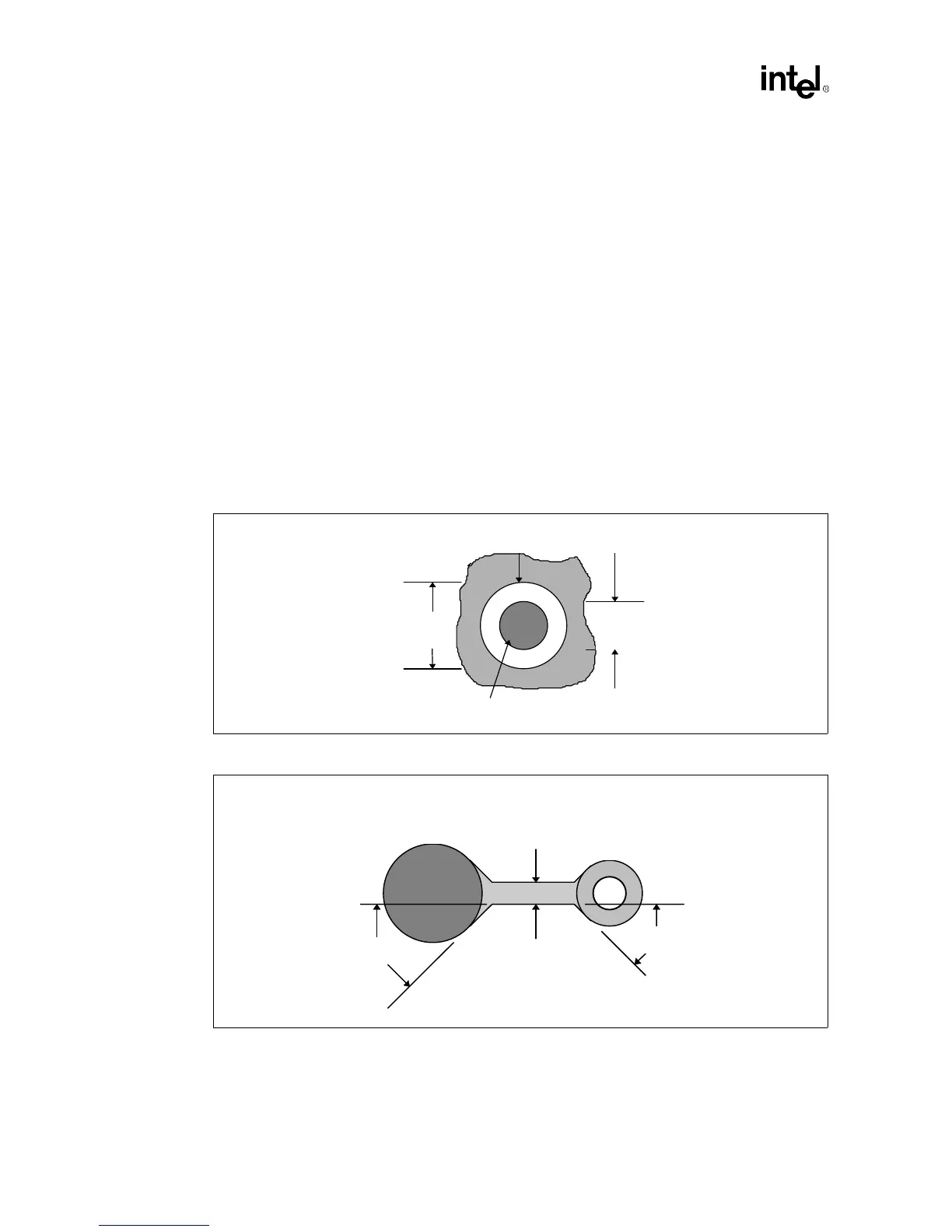
All non-ground BGA lands should be Metal Defined (MD) lands with the following nominal
dimensions (see Figure 2-6).
— Metal pad: 20 (6/6 routing) / 24 mils (5/5 routing)
— Solder mask opening: 24 mil (20 mil pad) / 27 mils (24 mil pad)
•
Any trace connected to a MBGA land or PTH via in the MBGA land grid array should be
teardropped. The teardrop should leave the trace at a 45° angle and intersect the via
tangentially (see Figure 2-7).
•
The minimum distance between the gold finger edge of the card and the center of the first row
of MBGA lands should be 525 mils, and 480 mils from the end of the start of the bevel.
•
All BGA ground vias should use 16 mil drill with no thermal reliefs.
Figure 2-6. Metal Defined land dimensions
Figure 2-7. BGA Trace
Solder Mask Opening
(.020”)
.024”
Metal Pad
(.024”)
.027”
Cover Trace with Solder Mask
BGA Land
PTH Via
.010” min
Recommended to be as
wide as via
45°
45°