•
RTS = Request to send
•
CTS = Clear to send
•
GND = Signal/Chassis Ground
The cable shield is to be grounded at both ends. For extremely EMC-prone environments, the GND may be
connected via a separate individually shielded wire pair to improve immunity to interference.
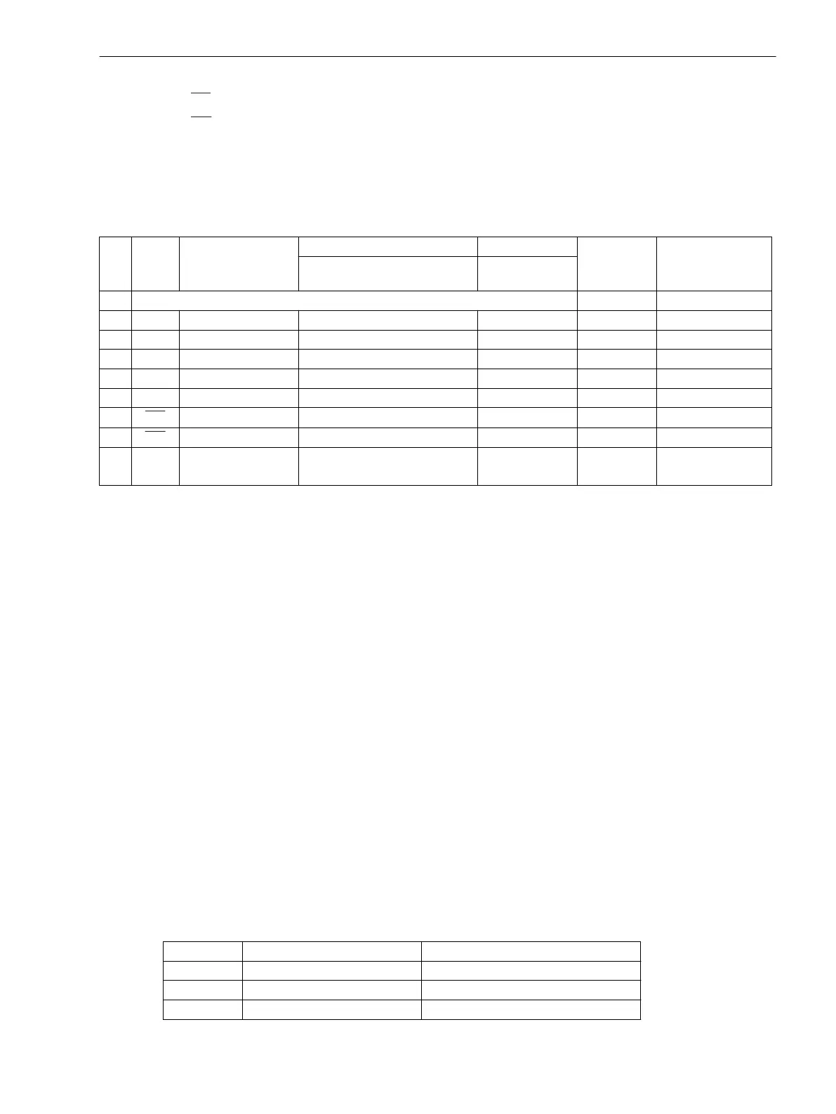
Table 3-31 Connector Assignment at the Various Interfaces
Pin-
No.
RS232 RS485 Profibus FMS Slave, RS485 Modbus RS485 EN 100
elektr.
RJ45
IEC 60870–5–103
redundant
RS485 (RJ45)
Profibus DP Slave, RS485 DNP 3.0 RS485
1 Shield (electrically connected with shield shroud) Tx+ B/B’ (RxD/TxD-P)
2 RxD – – – Tx– A/A’ (RxD/TxD-N)
3 TxD A/A’ (RxD/TxD-N) B/B’ (RxD/TxD-P) A Rx+
4 – – CNTR-A (TTL) RTS (TTL Pegel) –
5 GND C/C’ (GND) C/C’ (GND) GND1 –
6 – – +5 V (max. load with 100 mA) VCC1 Rx–
7 RTS
–
1)
– – –
8 CTS B/B’ (RxD/TxD-P) A/A’ (RxD/TxD-N) B –
9 – – – – not
provided
1)
Pin 7 also carries the RTS signal with RS232 level when operated as RS485 interface. Pin 7 must therefore
not be connected!
Additional Interface (only 7SJ64)
The additional interface (Port D), which is only available for 7SJ64, is used to connect signals from an RTD box.
The connection according to one of the connection examples given in Appendix C Connection Examples must
be verified. For the assignment of the connectors see the table above.
Termination
The RS485 interface is bus-capable for half-duplex operation with the signals A/A' and B/B' and the common
reference potential C/C' (GND). Verify that only at the bus of the last device the terminating resistors are
connected but not at the bus of the other devices.
The jumpers for the terminating resistors are located on the interface module RS485 (see Figure 3-22) or the
Profibus RS485 (see Figure 3-24). With 7SJ64 they are located directly on the C–CPU-2 (see Figure 3-15 and
Table 3-17).
The terminating resistors can also be connected externally (e.g. to the connection module, as illustrated in
Figure 3-16). In this case, the terminating resistors located on the module must be disconnected.
If the bus is extended, make sure again that only the last device on the bus has the terminating resistors
switched-in, and that all other devices on the bus do not.
Time Synchronization Interface
It is optionally possible to process 5 V-, 12 V- or 24 V- time synchronization signals, provided that they are
carried to the inputs named in the following table.
Table 3-32
D-SUB socket assignment of the time synchronization interface
Pin-No. Description Signal Meaning
1 P24_TSIG Input 24 V
2 P5_TSIG Input 5 V
3 M_TSIG Return Line
Mounting and Commissioning
3.2 Checking Connections
SIPROTEC 4, 7SJ62/64, Manual 413
C53000-G1140-C207-8, Edition 08.2016
 Loading...