Controller area network (bxCAN) RM0090
1098/1731 DocID018909 Rev 11
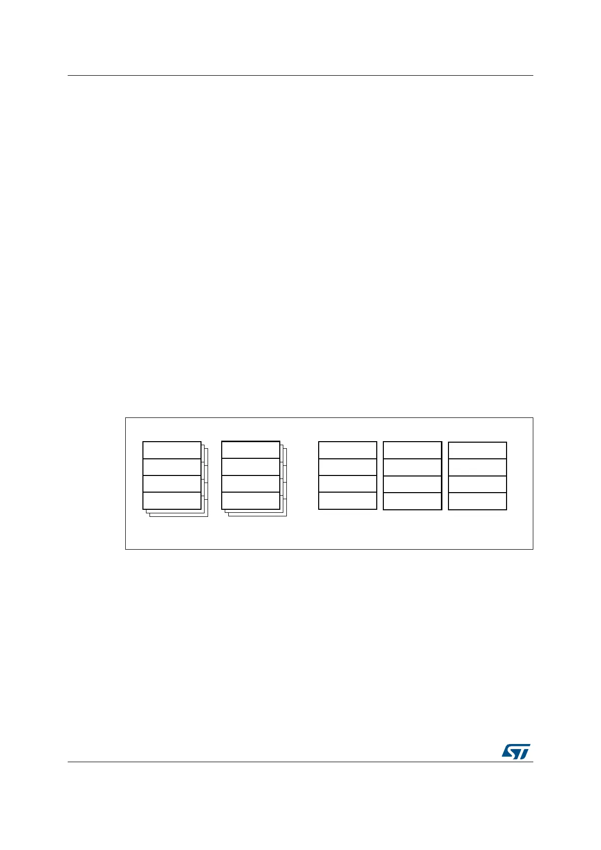
32.9.3 CAN mailbox registers
This chapter describes the registers of the transmit and receive mailboxes. Refer to
Section 32.7.5: Message storage on page 1082 for detailed register mapping.
Transmit and receive mailboxes have the same registers except:
• The FMI field in the CAN_RDTxR register.
• A receive mailbox is always write protected.
• A transmit mailbox is write-enabled only while empty, corresponding TME bit in the
CAN_TSR register set.
There are 3 TX Mailboxes and 2 RX Mailboxes. Each RX Mailbox allows access to a 3 level
depth FIFO, the access being offered only to the oldest received message in the FIFO.
Each mailbox consist of 4 registers.
Figure 349. RX and TX mailboxes
Bits 19:16 TS1[3:0]: Time segment 1
These bits define the number of time quanta in Time Segment 1
t
BS1
= t
q
x (TS1[3:0] + 1)
For more information on bit timing, please refer to Section 32.7.7: Bit timing on page 1084.
Bits 15:10 Reserved, must be kept at reset value.
Bits 9:0 BRP[9:0]
: Baud rate prescaler
These bits define the length of a time quanta.
t
q
= (BRP[9:0]+1) x t
PCLK
CAN_RI0R
CAN_RDT0R
CAN_RL0R
CAN_RH0R
CAN_TI0R
CAN_TDT0R
CAN_TDL0R
CAN_TDH0R
FIFO0
Three Tx Mailboxes
CAN_RI1R
CAN_RDT1R
CAN_RL1R
CAN_RH1R
FIFO1
CAN_TI1R
CAN_TDT1R
CAN_TDL1R
CAN_TDH1R
CAN_TI2R
CAN_TDT2R
CAN_TDL2R
CAN_TDH2R