Embedded Flash memory interface RM0090
74/1731 DocID018909 Rev 11
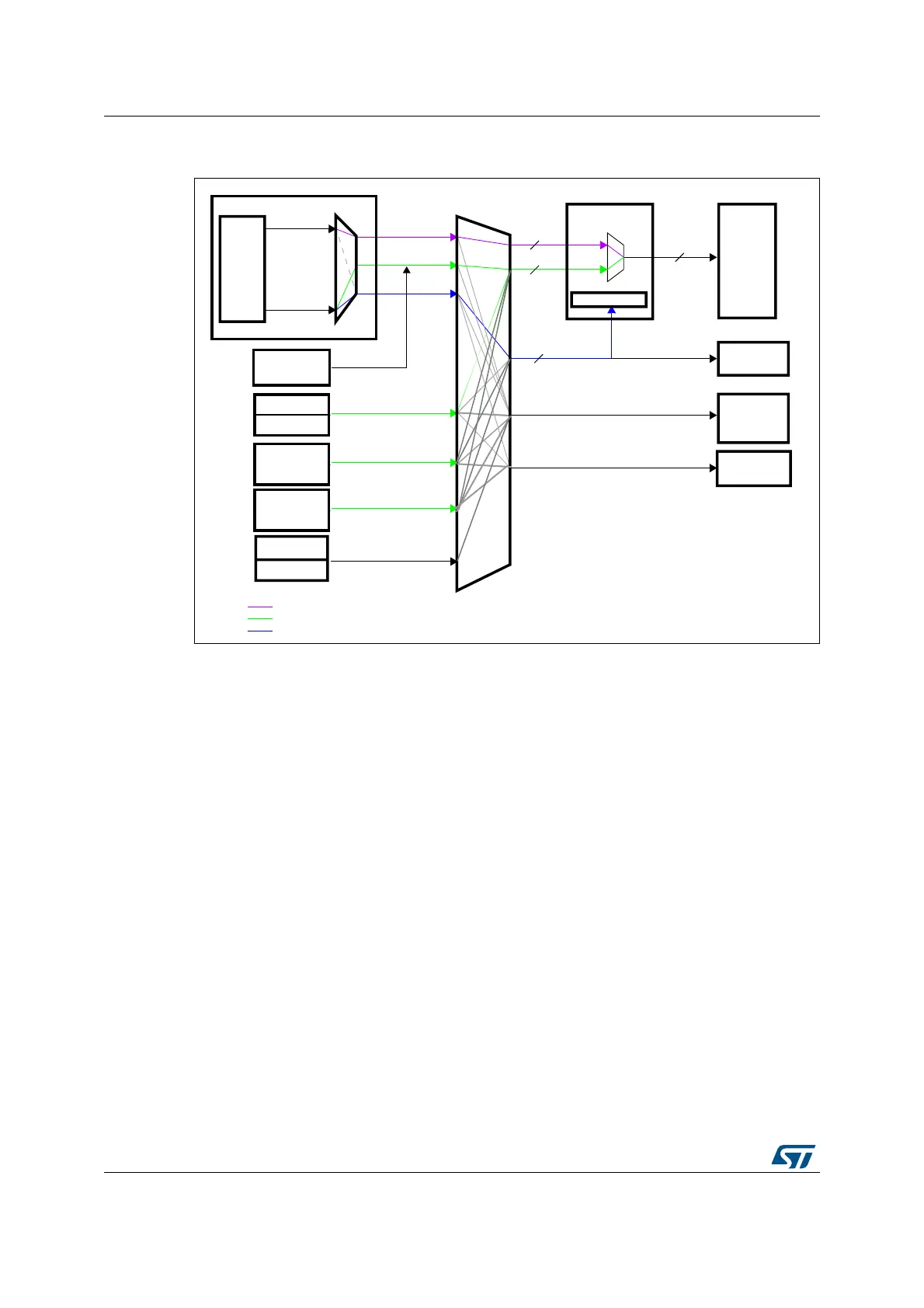
Figure 4. Flash memory interface connection inside system architecture
(STM32F42xxx and STM32F43xxx)
3.3 Embedded Flash memory in
STM32F405xx/07xx and STM32F415xx/17xx
The Flash memory has the following main features:
• Capacity up to 1 Mbyte
• 128 bits wide data read
• Byte, half-word, word and double word write
• Sector and mass erase
• Memory organization
The Flash memory is organized as follows:
– A main memory block divided into 4 sectors of 16 Kbytes, 1 sector of 64 Kbytes,
and 7 sectors of 128 Kbytes
– System memory from which the device boots in System memory boot mode
– 512 OTP (one-time programmable) bytes for user data
The OTP area contains 16 additional bytes used to lock the corresponding OTP
data block.
– Option bytes to configure read and write protection, BOR level, watchdog
software/hardware and reset when the device is in Standby or Stop mode.
• Low-power modes (for details refer to the Power control (PWR) section of the reference
manual)
#ORTEX
CORE
%THERNET
53"(3
$-!
$-!
$CODEBUS
)#ODEBUS
#ORTEX-WITH&05
)#ODE
$#ODE
3BUS
!("
PERIPH
&LASH
MEMORY
&LASHINTERFACE
32!-AND
EXTERNAL
MEMORIES
!("
PERIPH
&,)4®ISTERS
!("
BIT
INSTRUCTION
BUS
!CCESSTOINSTRUCTIONIN&LASHMEMORY
!CCESSTODATAANDLITERALPOOLIN&LASHMEMORY
&,)4®ISTERACCESS
-36
##-DATA
2!-
!("
BIT
DATABUS
!("
BIT
SYSTEMBUS
&LASH
MEMORY
BUS
BITS
$-!$
,#$4&4