Flexible memory controller (FMC) RM0090
1642/1731 DocID018909 Rev 11
FMC Bank 4 gives access to those 3 memory spaces as described in Section 37.4.2: NAND
Flash memory/PC Card address mapping and Table 251: NAND/PC Card memory mapping
and timing registers.
Wait feature
The CompactFlash or PC Card may request the FMC to extend the length of the access
phase programmed by MEMWAITx/ATTWAITx/IOWAITx bits, asserting the nWAIT signal
after nOE/nWE or nIORD/nIOWR activation if the wait feature is enabled through the
PWAITEN bit in the FMC_PCRx register. To detect correctly the nWAIT assertion, the
MEMWAITx/ATTWAITx/IOWAITx bits must be programmed as follows:
where max_wait_assertion_time is the maximum time taken by NWAIT to go low once
nOE/nWE or nIORD/nIOWR is low.
After WAIT de-assertion, the FMC extends the WAIT phase for 4 HCLK clock cycles.
37.6.8 NAND Flash/PC Card controller registers
PC Card/NAND Flash control registers 2..4 (FMC_PCR2..4)
Address offset: 0x40 + 0x20 * (x – 1), x = 2..4
Reset value: 0x0000 0018
X0 00101X-X0
Attribute
Space
Read or Write Configuration
Registers
YES
X0 00100X-X0
Read or Write CIS (Card
Information Structure)
YES
1 0 001XXX-X1
Attribute
Space
Invalid Read or Write (odd
address)
YES
0 1 001XXX-Xx
Invalid Read or Write (odd
address)
YES
1 0 010XXX-X0
I/O space
Read Even Byte on D7-0 YES
1 0 0 1 0 X X X-X 1 Read Odd Byte on D7-0 YES
1 0 0 1 0 X X X-X 0 Write Even Byte on D7-0 YES
1 0 0 1 0 X X X-X 1 Write Odd Byte on D7-0 YES
0 0 0 1 0 X X X-X 0 Read Word on D15-0 YES
0 0 0 1 0 X X X-X 0 Write word on D15-0 YES
0 1 0 1 0 X X X-X X Read Odd Byte on D15-8 Not supported
0 1 0 1 0 X X X-X X Write Odd Byte on D15-8 Not supported
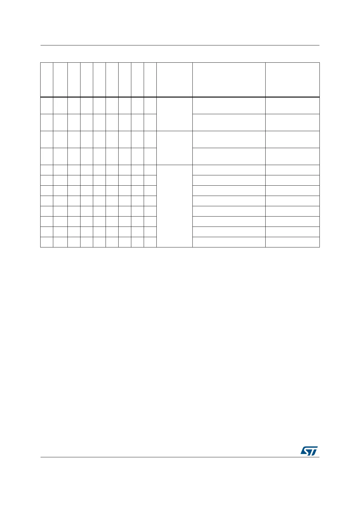
Table 289. 16-bit PC-Card signals and access type (continued)
nCE2
nCE1
nREG
nOE/nWE
nIORD
A10
A9
A7-1
A0
Space Access type
Allowed/not
Allowed
xxWAITx 4
max_wait_assertion_time
HCLK
-------------------------------------------------------------------+≥