DocID018909 Rev 11 1261/1731
RM0090 USB on-the-go full-speed (OTG_FS)
1368
Power and clock gating CSR map
There is a single register for power and clock gating. It is available in both host and device
modes.
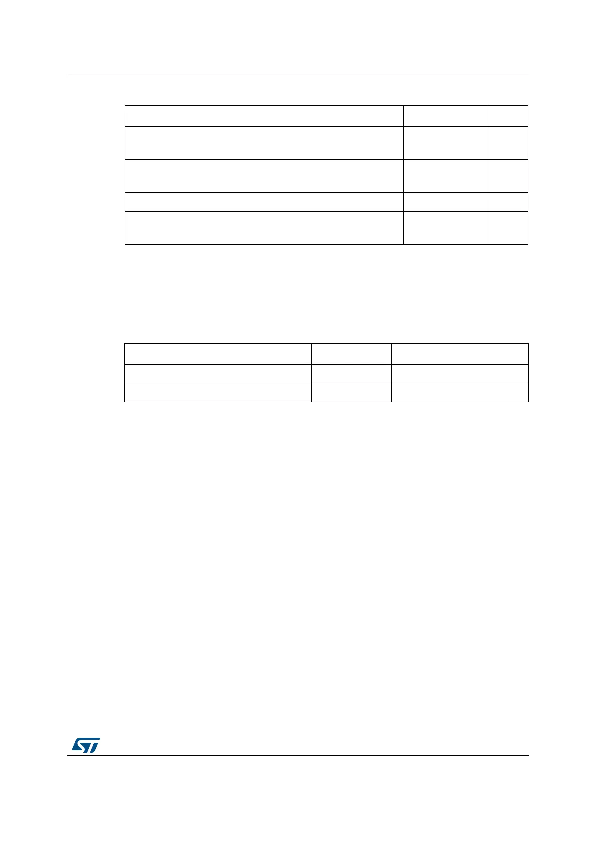
Table 198. Data FIFO (DFIFO) access register map
FIFO access register section Address range Access
Device IN Endpoint 0/Host OUT Channel 0: DFIFO Write Access
Device OUT Endpoint 0/Host IN Channel 0: DFIFO Read Access
0x1000–0x1FFC
w
r
Device IN Endpoint 1/Host OUT Channel 1: DFIFO Write Access
Device OUT Endpoint 1/Host IN Channel 1: DFIFO Read Access
0x2000–0x2FFC
w
r
... ... ...
Device IN Endpoint x
(1)
/Host OUT Channel x
(1)
: DFIFO Write Access
Device OUT Endpoint x
(1)
/Host IN Channel x
(1)
: DFIFO Read Access
1. Where x is 3 in device mode and 7 in host mode.
0xX000–0xXFFC
w
r
Table 199. Power and clock gating control and status registers
Register name Acronym Offset address: 0xE00–0xFFF
Power and clock gating control register PCGCR 0xE00-0xE04
Reserved 0xE05–0xFFF