DocID018909 Rev 11 1673/1731
RM0090 Debug support (DBG)
1701
38.4.1 SWJ debug port pins
Five pins are used as outputs from the STM32F4xx for the SWJ-DP as alternate functions of
general-purpose I/Os. These pins are available on all packages.
38.4.2 Flexible SWJ-DP pin assignment
After RESET (SYSRESETn or PORESETn), all five pins used for the SWJ-DP are assigned
as dedicated pins immediately usable by the debugger host (note that the trace outputs are
not assigned except if explicitly programmed by the debugger host).
However, the STM32F4xx MCUs offers the possibility of disabling some or all of the SWJ-
DP ports and so, of releasing the associated pins for general-purpose IO (GPIO) usage. For
more details on how to disable SWJ-DP port pins, please refer to
Section 8.3.2: I/O pin
multiplexer and mapping.
Note: When the APB bridge write buffer is full, it takes one extra APB cycle when writing the
GPIO_AFR register. This is because the deactivation of the JTAGSW pins is done in two
cycles to guarantee a clean level on the nTRST and TCK input signals of the core.
• Cycle 1: the JTAGSW input signals to the core are tied to 1 or 0 (to 1 for nTRST, TDI
and TMS, to 0 for TCK)
• Cycle 2: the GPIO controller takes the control signals of the SWJTAG IO pins (like
controls of direction, pull-up/down, Schmitt trigger activation, etc.).
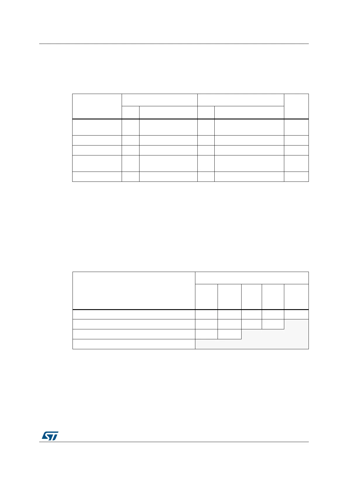
Table 293. SWJ debug port pins
SWJ-DP pin name
JTAG debug port SW debug port Pin
assign
ment
Type Description Type Debug assignment
JTMS/SWDIO I
JTAG Test Mode
Selection
IO
Serial Wire Data
Input/Output
PA13
JTCK/SWCLK I JTAG Test Clock I Serial Wire Clock PA14
JTDI I JTAG Test Data Input - - PA15
JTDO/TRACESWO O JTAG Test Data Output -
TRACESWO if async trace
is enabled
PB3
NJTRST I JTAG Test nReset - - PB4
Table 294. Flexible SWJ-DP pin assignment
Available debug ports
SWJ IO pin assigned
PA13 /
JTMS /
SWDIO
PA14 /
JTCK /
SWCLK
PA15 /
JTDI
PB3 /
JTDO
PB4 /
NJTRST
Full SWJ (JTAG-DP + SW-DP) - Reset State X X X X X
Full SWJ (JTAG-DP + SW-DP) but without NJTRST X X X X
JTAG-DP Disabled and SW-DP Enabled X X
JTAG-DP Disabled and SW-DP Disabled Released