Reset and clock control for STM32F42xxx and STM32F43xxx (RCC) RM0090
182/1731 DocID018909 Rev 11
6.3.11 RCC AHB2 peripheral clock enable register (RCC_AHB2ENR)
Address offset: 0x34
Reset value: 0x0000 0000
Access: no wait state, word, half-word and byte access.
Bit 5 GPIOFEN: IO port F clock enable
This bit is set and cleared by software.
0: IO port F clock disabled
1: IO port F clock enabled
Bit 4 GPIOEEN: IO port E clock enable
This bit is set and cleared by software.
0: IO port E clock disabled
1: IO port E clock enabled
Bit 3 GPIODEN: IO port D clock enable
This bit is set and cleared by software.
0: IO port D clock disabled
1: IO port D clock enabled
Bit 2 GPIOCEN: IO port C clock enable
This bit is set and cleared by software.
0: IO port C clock disabled
1: IO port C clock enabled
Bit 1 GPIOBEN: IO port B clock enable
This bit is set and cleared by software.
0: IO port B clock disabled
1: IO port B clock enabled
Bit 0 GPIOAEN: IO port A clock enable
This bit is set and cleared by software.
0: IO port A clock disabled
1: IO port A clock enabled
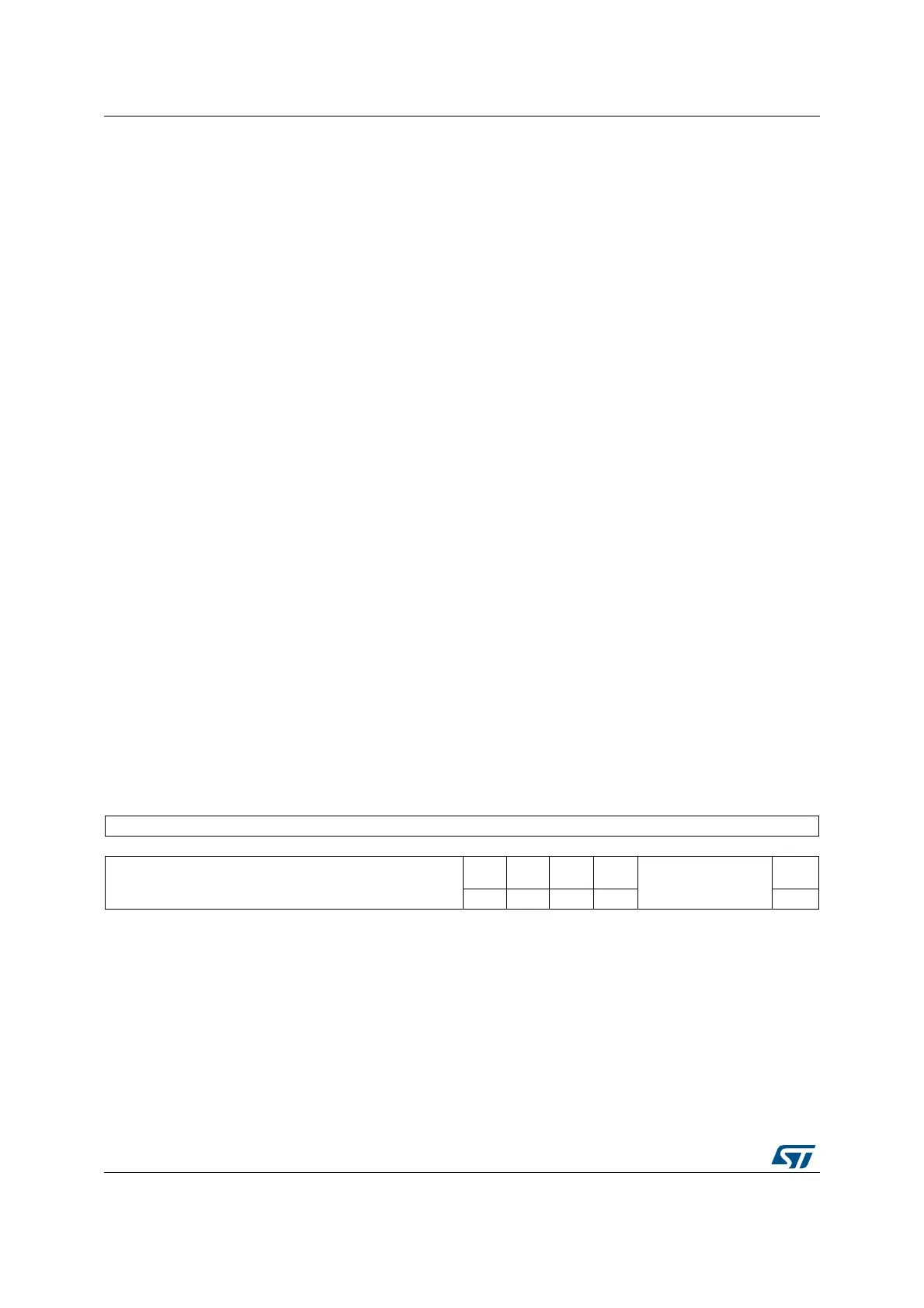
31 30 29 28 27 26 25 24 23 22 21 20 19 18 17 16
Reserved
15 14 13 12 11 10 9 8 7 6 5 4 3 2 1 0
Reserved
OTGFS
EN
RNG
EN
HASH
EN
CRYP
EN
Reserved
DCMI
EN
rw rw rw rw rw
Bits 31:8 Reserved, must be kept at reset value.
Bit 7 OTGFSEN: USB OTG FS clock enable
This bit is set and cleared by software.
0: USB OTG FS clock disabled
1: USB OTG FS clock enabled
Bit 6 RNGEN: Random number generator clock enable
This bit is set and cleared by software.
0: Random number generator clock disabled
1: Random number generator clock enabled