Digital camera interface (DCMI) RM0090
468/1731 DocID018909 Rev 11
15.8 DCMI register description
All DCMI registers have to be accessed as 32-bit words, otherwise a bus error occurs.
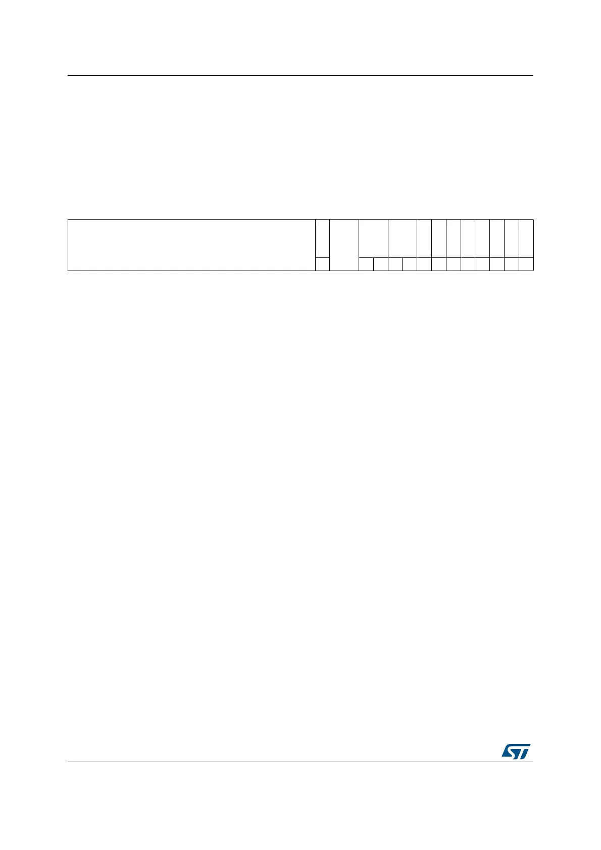
15.8.1 DCMI control register 1 (DCMI_CR)
Address offset: 0x00
Reset value: 0x0000 0x0000
313029282726252423222120191817161514131211109876543210
Reserved
ENABLE
Reserved
EDM FCRC
VSPOL
HSPOL
PCKPOL
ESS
JPEG
CROP
CM
CAPTURE
rw rw rw rw rw rw rw rw rw rw rw rw rw
Bit 31:15 Reserved, must be kept at reset value.
Bit 14 ENABLE: DCMI enable
0: DCMI disabled
1: DCMI enabled
Note: The DCMI configuration registers should be programmed correctly before
enabling this Bit
Bit 13: 12 Reserved, must be kept at reset value.
Bits 11:10 EDM[1:0]: Extended data mode
00: Interface captures 8-bit data on every pixel clock
01: Interface captures 10-bit data on every pixel clock
10: Interface captures 12-bit data on every pixel clock
11: Interface captures 14-bit data on every pixel clock
Bits 9:8 FCRC[1:0]: Frame capture rate control
These bits define the frequency of frame capture. They are meaningful only in
Continuous grab mode. They are ignored in snapshot mode.
00: All frames are captured
01: Every alternate frame captured (50% bandwidth reduction)
10: One frame in 4 frames captured (75% bandwidth reduction)
11: reserved
Bit 7 VSPOL: Vertical synchronization polarity
This bit indicates the level on the VSYNC pin when the data are not valid on the
parallel interface.
0: VSYNC active low
1: VSYNC active high
Bit 6 HSPOL: Horizontal synchronization polarity
This bit indicates the level on the HSYNC pin when the data are not valid on the
parallel interface.
0: HSYNC active low
1: HSYNC active high
Bit 5 PCKPOL: Pixel clock polarity
This bit configures the capture edge of the pixel clock
0: Falling edge active.
1: Rising edge active.