DocID018909 Rev 11 297/1731
RM0090 System configuration controller (SYSCFG)
303
There are two possible FMC remap at address 0x0000 0000:
• FMC Bank 1 (NOR/PSRAM 1 and 2) remap:
Only the first two regions of Bank 1 memory controller (Bank1 NOR/PSRAM 1 and
NOR/PSRAM 2) can be remapped.
• FMC SDRAM Bank 1 remap.
In remap mode at address 0x0000 0000, the CPU can access the external memory via
ICode bus instead of System bus which boosts up the performance.
Address offset: 0x00
Reset value: 0x0000 000X (X is the memory mode selected by the BOOT pins)
Note: Booting from NOR Flash memory or SDRAM is not allowed. The regions can only be
mapped at 0x0000 0000 through software remap.
)
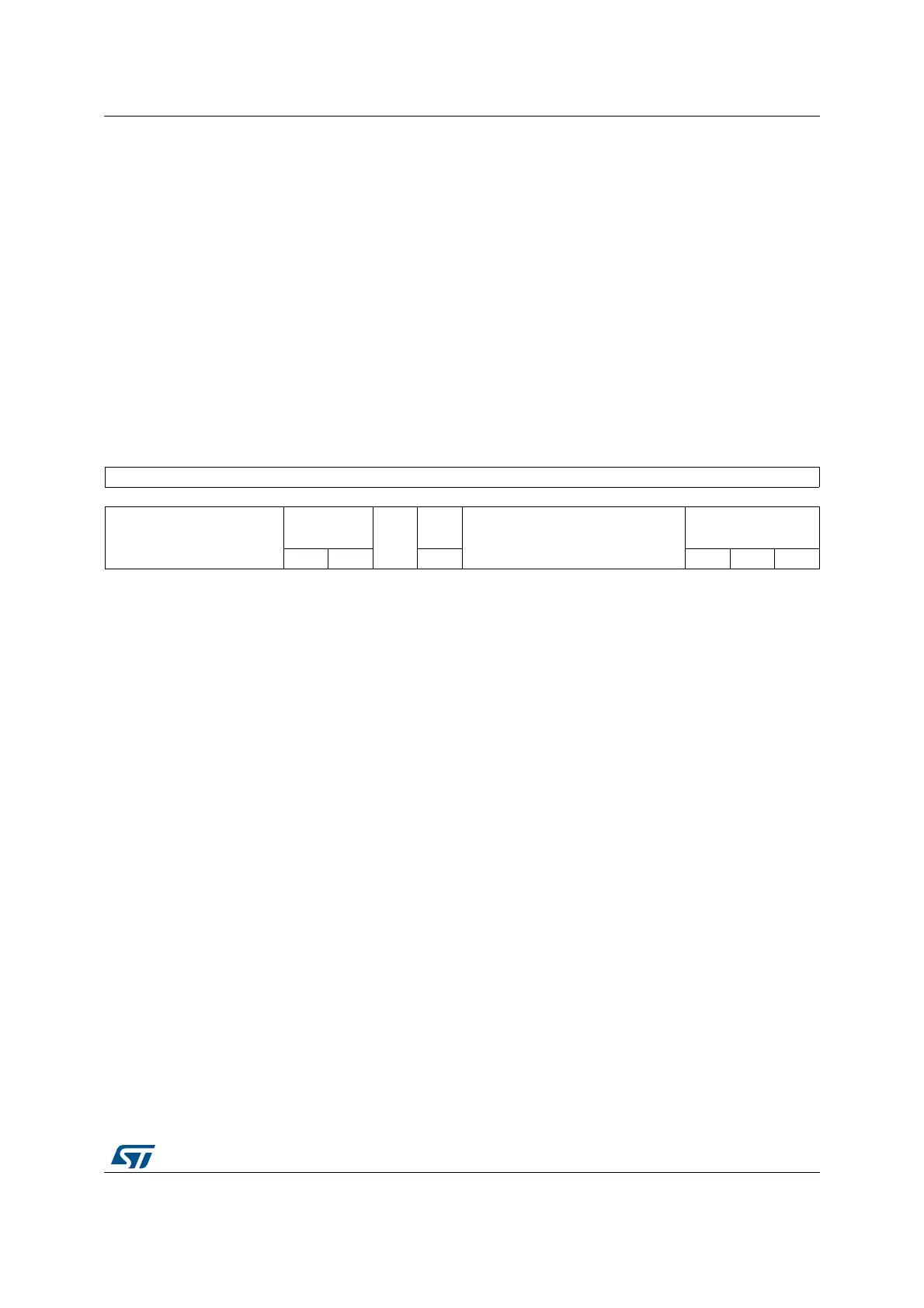
31 30 29 28 27 26 25 24 23 22 21 20 19 18 17 16
Reserved
1514131211109876543210
Reserved
SWP_FMC
Res.
FB_
MODE
Reserved
MEM_MODE[2:0]
rw rw rw rw rw rw
Bits 31:12 Reserved, must be kept at reset value.
Bits 11:10 SWP_FMC: FMC memory mapping swap
Set and cleared by software. These bits are used to swap the FMC SDRAM
Bank 1/2 and FMC Bank 3/4 (SDRAM Bank 1/2 and NAND Bank 2/PCCARD
Bank) in order to enable the code execution from SDRAM Banks without a
physical remapping at 0x0000 0000 address.
00: No FMC memory mapping swap
01: SDRAM banks and NAND Bank 2/PCCARD mapping are swapped. SDRAM
Bank 1 and 2 are mapped at NAND Bank 2 (0x8000 0000) and PCCARD Bank
(0x9000 0000) address, respectively. NAND Bank 2 and PCCARD Bank are
mapped at 0xC000 0000 and 0xD000 0000, respectively.
10: Reserved
11: Reserved
Bit 9 Reserved, must be kept at reset value.