Active
state
state
Standby
state
Sleep
Delay
FACTIVEWAIT
cycles
Delay
FSTDBYWAIT
cycles
FSTDBYWAIT
cycles
FACTIVEWAIT
Delay
cycles
Delay
Highest
power
Lowest power
Longest
Wake up time
PWR=0,1
PWR=0,0
PWR=0,0
PWR=1,1
or access to
the Flash/OTP
PWR=0,1
PWR=1,1
or access to
the Flash/OTP
Reset
www.ti.com
Flash and OTP Power Modes
Note: During the boot process, the Boot ROM performs a dummy read of the Code Security
Module (CSM) password locations located in the flash. This read is performed to unlock a
new or erased device that has no password stored in it so that flash programming or loading
of code into CSM protected SARAM can be performed. On devices with a password stored,
this read has no affect and the CSM remains locked (see Chapter 2 for information on the
CSM). One effect of this read is that the flash will transition from the sleep (reset) state to the
active state.
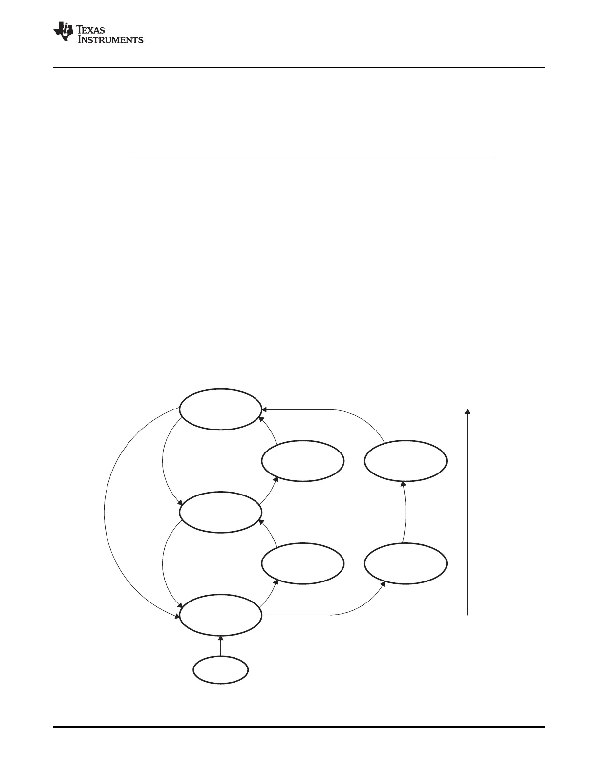
The flash/OTP bank and pump are always in the same power mode. See Figure 1-1 for a graphic
depiction of the available power states. You can change the current flash/OTP memory power state as
follows:
• To move to a lower power state
Change the PWR mode bits from a higher power mode to a lower power mode. This change
instantaneously moves the flash/OTP bank to the lower power state. This register should be accessed
only by code running outside the flash/OTP memory.
• To move to a higher power state
To move from a lower power state to a higher power state, there are two options.
1. Change the FPWR register from a lower state to a higher state. This access brings the flash/OTP
memory to the higher state.
2. Access the flash or OTP memory by a read access or program opcode fetch access. This access
automatically brings the flash/OTP memory to the active state.
There is a delay when moving from a lower power state to a higher one. See Figure 1-1 . This delay is
required to allow the flash to stabilize at the higher power mode. If any access to the flash/OTP memory
occurs during this delay the CPU automatically stalls until the delay is complete.
Figure 1-1. Flash Power Mode State Diagram
SPRUFB0C – September 2007 – Revised May 2009 Flash and OTP Memory Blocks 17
Submit Documentation Feedback
 Loading...