D300529 0115 - BL67 I/O modules
12-81
BL67-1CNT/ENC
Process output/control interface
X = reserved
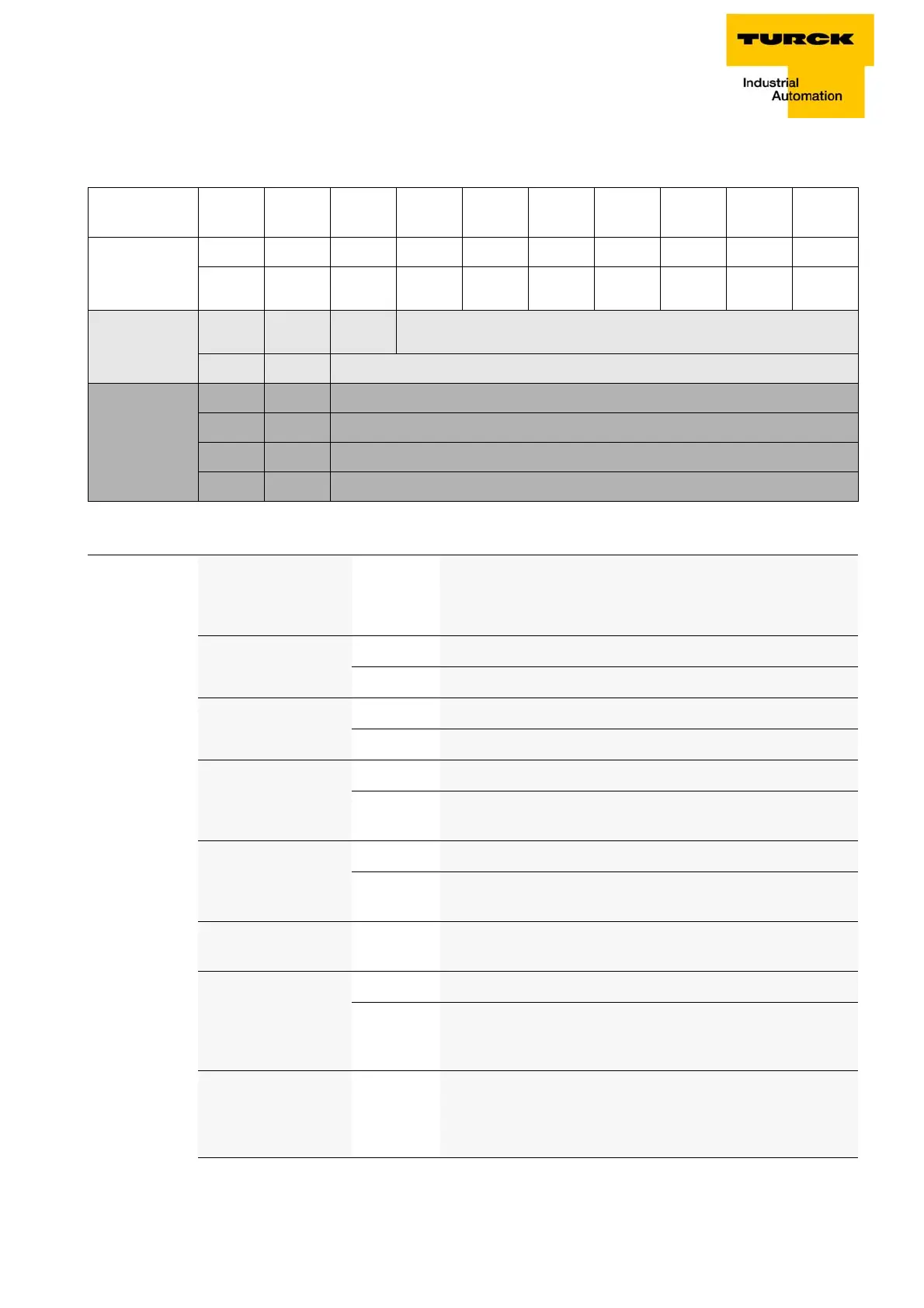
Byte Byte
in DP
Bit 7 Bit 6 Bit 5 Bit 4 Bit 3 Bit 2 Bit 1 Bit 0
Control bytes
0 7 DO3 DO2 DO1 DO0 X X X GATE
16X
SYNC_
REQ
XXXXX
RES_
STS
Communication
2 5
REG_
WR
REG_WR_ADR
3 4 REG_RD_ADR
user data
4 3 REG_WR_DATA, byte 0
5 2 REG_WR_DATA, byte 1
6 1 REG_WR_DATA, byte 2
7 0 REG_WR_DATA, byte 3
Table 12-9:
Process output
data of the mod-
ule
Bit Value Meaning
GATE 0 Counter inactive
1
Counter active, depending on parameter Gate function
DO0 to DO3 0 Digital output DOx = 0
1
Digital output DOx = 1
RES_STS 0 inactive
1
During the change from 0 to 1 the counter status bits (STS_U-
FLW and STS_OFLW) are reset.
SYNC_REQ 0 no synchronization
1
synchronization request
→ The bit SYNC_AKN of the status interface is reset.
REG_WR_ADR 0 to 127 Address of the register which has to be written with REG_WR_-
DATA.
REG_WR 0 Initial state
1
Write register
→ Command to overwrite the content of register of the
address REG_WR_ADR with REG_WR_DATA.
REG_RD_ADR 0 to 127 Address of the register which has to be read. If RD_ABORT = 0,
the user data can be found in REG_RD_DATA in the status inter-
face
(bytes 4-7).