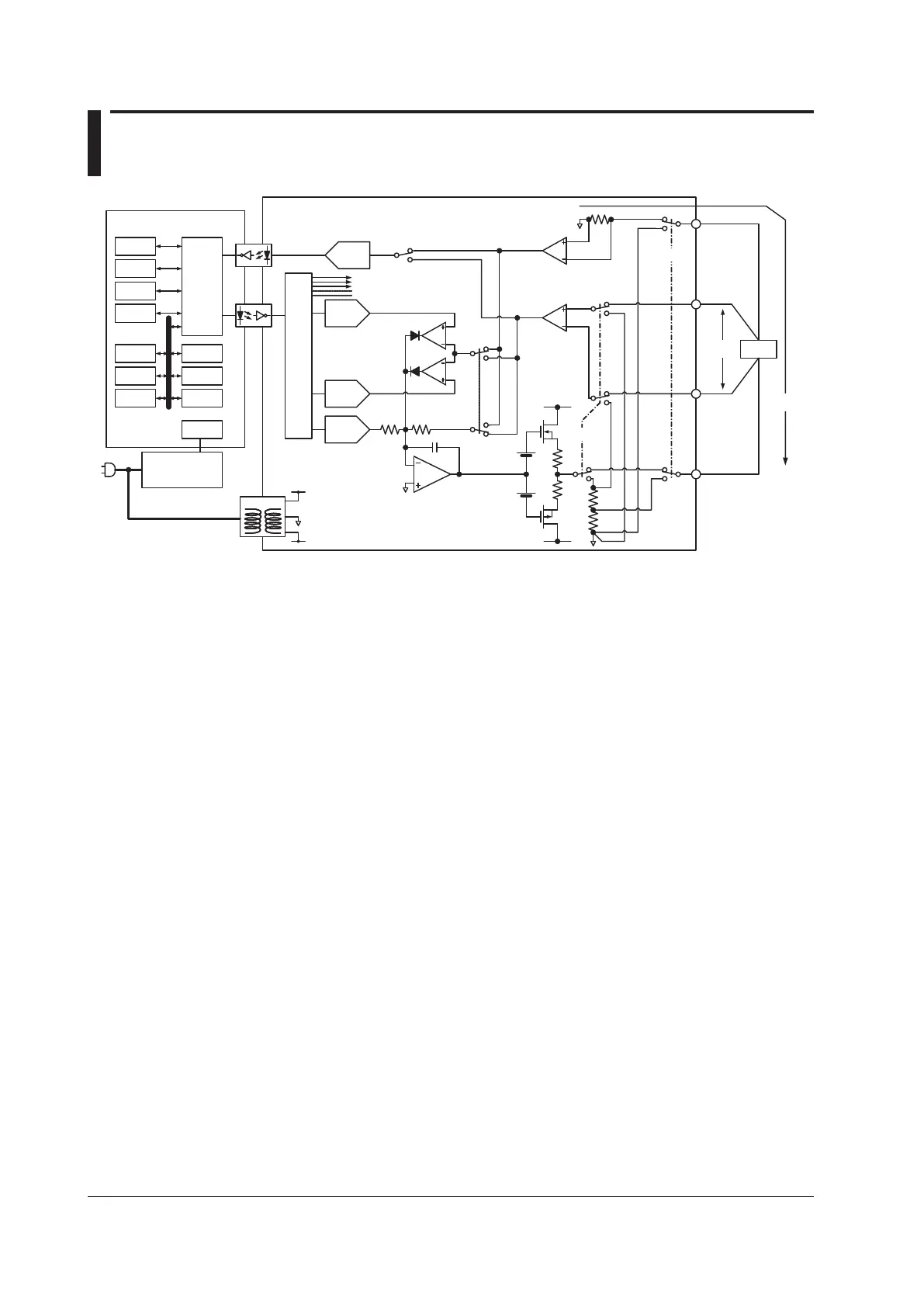
Appendix 2 Block Diagram
VFD
LED
KEY
GP-IB I/F
LAN I/F
SYNC I/F
FPGA
SDRAM
CPU
DC/DC
Power Supply
AC/DC
USB I/F
AC/DC
ADC
+Limit
DAC
-Limit
DAC
Source
DAC
PLD
Rs
DUT
Vo
(VL)
Io
(IL)
Power AMP
SW1
V
I
V
I
Vp
Vm
Vs
R1 R2
V/I
mV
V/I
mV
V/I
V/I
mV
mV
V/I
mV
SW2
SW2
R3
R4
FLASH ROM
Switch
Control
Current
Sense
Voltage
Sense
SENSE Hi
OUTPUT Hi
OUTPUT Lo
SENSE Lo
Limiter
Analog section
Digital section
The GS200 consists of a digital section that operates at ground potential and an
analog section that is isolated from the digital section. The digital section consists of a
CPU, FPGA, memory, and various interface circuits. A non-isolated DC-DC converter
supplies power to the digital section. The digital section controls the display, keys,
communications, and the analog section.
The analog section consists of the voltage source’s D/A converters (DACs), an output
amplifier, highly stable shunt resistors, and a limiter circuit. An isolated commercial
transformer provides power to the analog section.
Data that is sent from the digital section passes through a photocoupler and the PLD and
controls each DAC and the various switches that are used for making range settings and
other settings.
When the GS200 is operating as a voltage source, SW1 is connected to V, and source
voltage Vo is the product of source DAC value Vs and R2/R1. If load current IL increases
positively and IL × Rs exceeds positive limiter DAC value Vp, the diode of the limiter
circuit will turn on and suppress the load current to Vp/Rs. A similar operation takes place
when the load current is negative.
When the GS200 is operating as a current source, SW1 is connected to I, and source
current Io is the product of source DAC value Vs and (R2/R1)/Rs. If load voltage VL
exceeds positive limiter DAC value Vp, the diode of the limiter circuit will turn on and
suppress the load voltage to Vp. A similar operation takes place when the load voltage is
negative.
The GS200 is equipped with a measurement circuit that is separate from the source and
limiter circuits. In voltage source mode, the measurement circuit uses A/D converters
(ADC) to measure the current that is received. In current source mode, the measurement
circuit uses A/D converters (ADC) to measure the voltage that is received. Differing
from the voltage and current source functions described above, when the mV range is
selected in voltage source mode, SW2 is connected to mV. The source voltage Vo is
voltage-divided by R3 and R4. In this situation, because the output resistance becomes
R4 (2
Ω
), if the DUT does not have a high impedance, the source voltage is reduced
according to the DUT’s impedance. Additionally, because selecting mV causes the limiter
and current measurement circuits to be disconnected by Rs and SW2 that are used for
current sense, these circuits do not operate.
App-2
IM GS210-01EN
 Loading...