Debug
ARM DDI 0388I Copyright © 2008-2012 ARM. All rights reserved. 10-16
ID073015 Non-Confidential
10.8 External debug interface
The system can access memory-mapped debug registers through the Cortex-A9 APB slave port.
This APB slave interface supports 32-bits wide data, stalls, slave-generated aborts, and 11
address bits [12:2] mapping 2x4KB of memory. bit [12] of PADDRDBG[12:0] selects which
of the components is accessed:
•Use PADDRDBG[12] = 0 to access the debug area of the Cortex-A9 processor. See
Table 10-1 on page 10-5 for debug resources memory mapping.
•Use PADDRDBG[12] = 1 to access the PMU area of the Cortex-A9 processor. See
Table 11-1 on page 11-3 for PMU resources memory mapping.
The PADDRDBG31 signal indicates to the processor the source of the access.
See Appendix A Signal Descriptions for a complete list of the external debug signals.
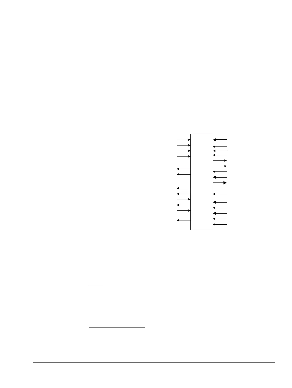
Figure 10-5 shows the external debug interface signals.
Figure 10-5 External debug interface signals
10.8.1 Debugging modes
Authentication signals control the debugging modes. The authentication signals configure the
processor so its activity can only be debugged or traced in a certain subset of processor modes
and security states. See Authentication signals on page 10-17.
The Cortex-A9 processor only supports halting debug-mode debugging in secure User mode
when invasive debugging is enabled by the SPIDEN pin. When SPIDEN is LOW, only monitor
mode debugging in secure User mode is available by setting the SDR.SUIDEN bit. That is,
when SPIDEN is LOW, the processor is not permitted to enter Halting Debug Mode even if the
SDR.SUIDEN bit is set to 1. You can bypass this restriction by setting the external SPIDEN pin
HIGH.
Cortex-A9
processor
SPIDEN
SPNIDEN
DBGEN
NIDEN
COMMTX
COMMRX
DBGCPUDONE
DBGRESTARTED
DBGNOPWRDWN
DBGACK
EDBGRQ
DBGRESTART
PSELDBG
PADDRDBG[12:2]
PRDATADBG[31:0]
PENABLEDBG
PREADYDBG
PSLVERRDBG
PWRITEDBG
DBGROMADDR[31:12]
DBGROMADDRV
DBGSELFADDR[31:15]
DBGSELFADDRV
DBGSWENABLE
PWDATADBG[31:0]
nDBGRESET
PADDRDBG31