Functional Description
ARM DDI 0388I Copyright © 2008-2012 ARM. All rights reserved. 2-6
ID073015 Non-Confidential
2.3 Clocking and resets
This section describes the clocks and resets of the processor in:
• Synchronous clocking
• Reset
• Dynamic high level clock gating on page 2-8.
2.3.1 Synchronous clocking
The Cortex-A9 uniprocessor has one functional clock input, CLK.
The Cortex-A9 uniprocessor does not have any asynchronous interfaces. All the bus interfaces
and the interrupt signals must be synchronous with reference to CLK.
The AXI bus clock domain can be run at n:1 (AXI: processor ratio to CLK) using the ACLKEN
signal.
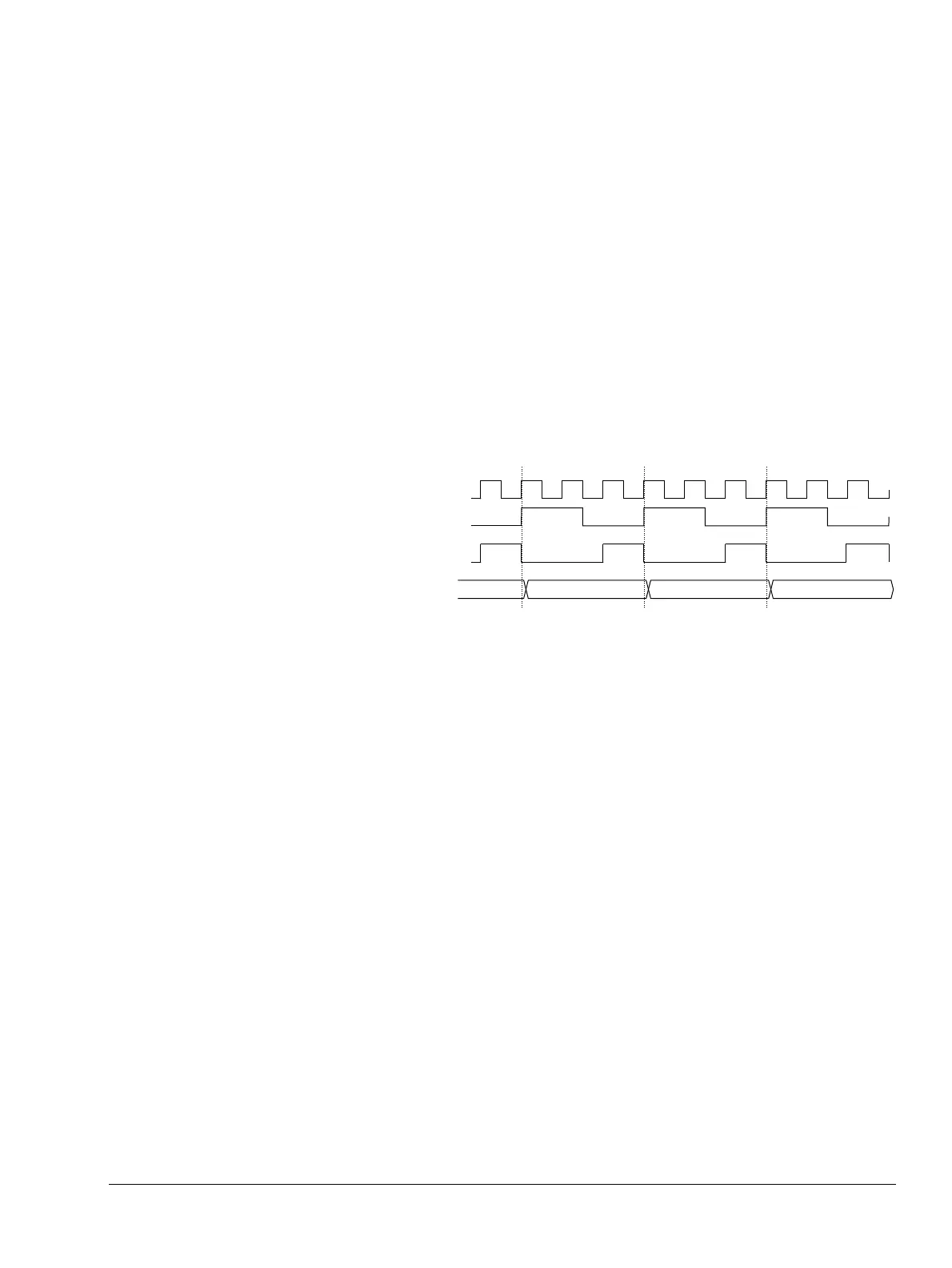
Figure 2-3 shows a timing example with ACKLENM0 used with a 3:1 clock ratio between
CLK and ACLK in a Cortex-A9 uniprocessor.
Figure 2-3 ACLKENM0 used with a 3:1 clock ratio
The master port, Master0, changes the AXI outputs only on the CLK rising edge when
ACLKENM0 is HIGH.
2.3.2 Reset
The Cortex-A9 processor has the following reset inputs:
nCPURESET The nCPURESET signal is the main Cortex-A9 processor reset. It
initializes the Cortex-A9 processor logic and the FPU logic including the
FPU register file when the MPE or FPU option is present.
nNEONRESET The nNEONRESET signal is the reset that controls the NEON SIMD
independently of the main Cortex-A9 processor reset.
nDBGRESET The nDBGRESET signal is the reset that initializes the debug logic. See
Chapter 10 Debug.
All of these are active-LOW signals.
Address1 Address2 Address3
CLK
ACLK
ACLKENM0
ARRDRM0 Address0