Debug
ARM DDI 0388I Copyright © 2008-2012 ARM. All rights reserved. 10-19
ID073015 Non-Confidential
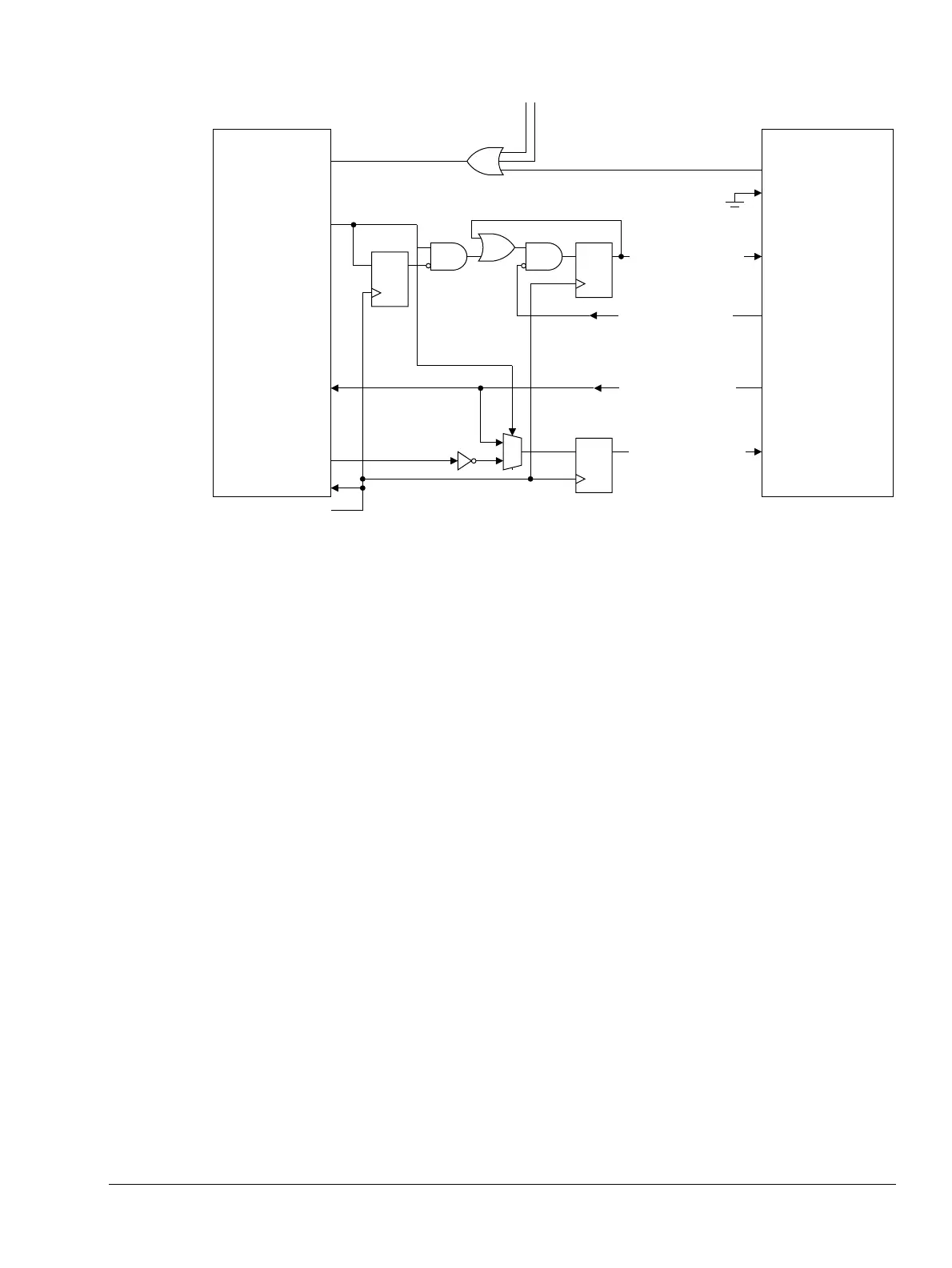
Figure 10-6 Debug request restart-specific connections
COMMRX and COMMTX
The COMMRX and COMMTX output signals enable interrupt-driven communications over
the DTR. By connecting these signals to an interrupt controller, software using the debug
communications channel can be interrupted whenever there is new data on the channel or when
the channel is clear for transmission.
COMMRX is asserted when the CP14 DTR has data for the processor to read, and it is
deasserted when the processor reads the data. Its value is equal to the DBGDSCR[30] DTRRX
full flag.
COMMTX is asserted when the CP14 is ready for write data, and it is deasserted when the
processor writes the data. Its value ia equal to the inverse of the DBGDSCR[29] DTRTX full
flag.
DBGROMADDR, and DBGSELFADDR
The Cortex-A9 processor has a memory-mapped debug interface. The processor can access the
debug and PMU registers by executing load and store instructions through the AXI bus.
DBGROMADDR gives the base address for the ROM table that locates the physical addresses
of the debug components.
DBGSELFADDR gives the offset from the ROM table to the physical addresses of the
processor registers.
DQ
DBGTRIGGERREQ
DBGTRIGGERACK
Processor CLK
CTITRIGIN[0]
CTITRIGINACK[0]
EDBGRQ CTITRIGOUT[0]
CTITRIGOUTACK[0]
DBGRESTARTED
CTITRIGOUTACK[7]
DBGRESTART
CTITRIGOUT[7]
CPU0 CTI0
DBGACK
0
1
DBGRESTARTACK
DQ
DBGRESTARTREQ
DQ