Operating Principles
EPSON Stylus Color 3000 Service Manual
2-14
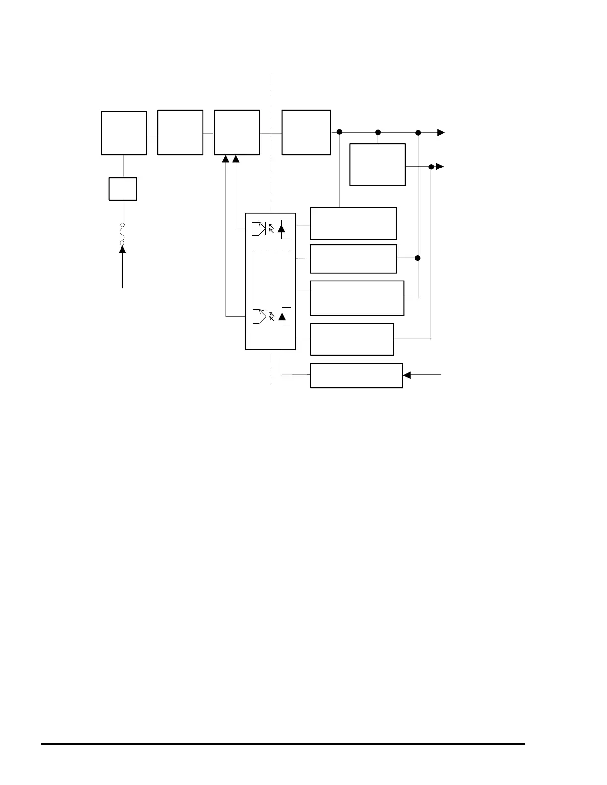
Figure 2-14 illustrates the electrical circuit diagram.
+5 VDC line overvoltage protection circuit
The output voltage level of the +5 V line is monitored by a Zener diode (ZD53). If the voltage level exceeds
+9 V, the status is fed back to the primary switching circuit through the transistor (Q82) and photocoupler
(PC1) to cut off the +42 V line to the regulator (IC51).
+5 VDC line constant voltage control circuit
Voltage at the +5 VDC line is controlled by the regulator IC (IC51). When abnormal voltage at the +5 VDC
line is detected, the status is input to the internal comparator of the regulator, controlling the voltage.
+42 VDC line overvoltage protection circuit
The output level of the +42 VDC line is monitored by the 2 Zener diodes ZD52 and ZD87. When the output
level of the +42 VDC line exceeds +48 V, the switching FET operation on the primary side is stopped via the
thyristor (CY52), transistor (Q81), and photocoupler (PC1).
+42 VDC line constant voltage control circuit
Voltage at the +42 VDC line is monitored by the Zener diodes (ZD51, ZD81−ZD86). This circuit feeds the
output voltage level status through a photocoupler (PC1) to the primary switching circuit to control the
switching FET to produce a constant output voltage level.
+42 VDC line overcurrent protection circuit
Output current is monitored by transistors Q81 and Q82. If the measured output current is abnormally low,
there is a short circuit, and the overprotection circuit has fed back to the primary circuit to stop the switching
FET operation.
Full Wave
Rectifier
Circuit
Filter
Fuse
AC Input
Smoothing
Circuit
Switching
Circuit
(Q1)
Half Wave
Rectifier
Circuit
Chopping
Regulator
(IC51)
+42 V
Line Constant
Voltage Control Circuit
(ZD51, 81 to 86)
+42 V
Line Overcurrent
Protection Circuit
(Q81, Q82)
+5 V
Overvoltage
Protection Circuit
(ZD53, Q82)
Power Off Delay Circuit
(ZD88, C84, Q84)
Primary Circuit
Secondary Circuit
+42 V
+5 V
Power Off Signal
Photo-coupler
PC1
+42 V
Line Overvoltage
Protection Circuit
(ZD52, ZD87, Q81)
Figure 2-14. Power Supply Circuit Diagram
 Loading...